SBOSA86 March 2023 INA310A , INA310B
PRODUCTION DATA
- 1 Features
- 2 Applications
- 3 Description
- 4 Revision History
- 5 Pin Configuration and Functions
- 6 Specifications
- 7 Detailed Description
- 8 Application and Implementation
- 9 Device and Documentation Support
- 10Mechanical, Packaging, and Orderable Information
Package Options
Mechanical Data (Package|Pins)
- DGK|8
Thermal pad, mechanical data (Package|Pins)
Orderable Information
6.6 Typical Characteristics
at TA = 25°C, VS = 5 V, VSENSE = VIN+ – VIN– = 0.5 V / Gain, VCM = VIN– = 48 V, and RPULLUP= 5.1 kΩ (unless otherwise noted).
 Figure 6-1 INA310A1 Input Offset Production Distribution
 Figure 6-3 INA310A3 Input Offset Production Distribution
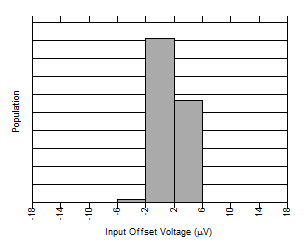 Figure 6-5 INA310A5 Input Offset Production Distribution
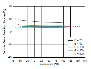 Figure 6-7 Common-Mode
Rejection Ratio vs Temperature
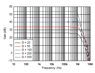 Figure 6-9 Gain vs
Frequency
 Figure 6-11 Power-Supply
Rejection Ratio vs Temperature
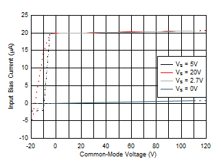
| VSENSE = 0 V |
 Figure 6-15 INA310x1 Input Bias Current vs VSENSE
| VS = 5 V |
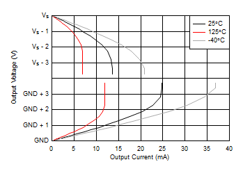
 Figure 6-21 Output
Impedance vs Frequency
 Figure 6-23 Swing to GND vs
Temperature
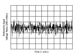 Figure 6-25 Input Referred
Noise
Figure 6-27 Quiescent Current vs Temperature

Figure 6-29 Quiescent Current vs Common-Mode Voltage
 Figure 6-31 INA310x3 Step Response
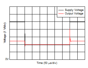

Figure 6-35 Comparator Trip Point vs Supply Voltage

Figure 6-37 Comparator Propagation Delay vs Overdrive Voltage

Figure 6-39 Comparator Propagation Delay vs Temperature
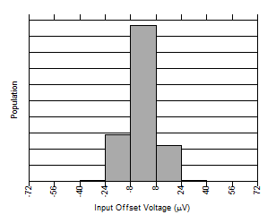 Figure 6-2 INA310A2 Input Offset Production Distribution
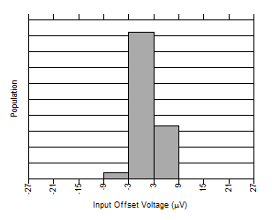 Figure 6-4 INA310A4 Input Offset Production Distribution
 Figure 6-6 Input Offset
Voltage vs Temperature
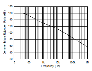 Figure 6-8 Common-Mode
Rejection Ratio vs Frequency
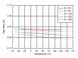 Figure 6-10 INA310A Gain Error vs Temperature
 Figure 6-12 Power-Supply
Rejection Ratio vs Frequency
 Figure 6-16 INA310x2, INA310x3 Input Bias Current vs VSENSE
| VS = 2.7 V |
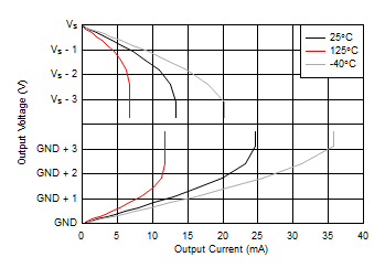
| VS = 20 V |
 Figure 6-22 Swing to Supply
vs Temperature
 Figure 6-24 Input Referred
Noise vs Frequency
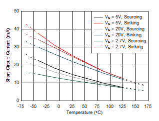 Figure 6-26 Short-Circuit
Current vs Temperature
Figure 6-28 Quiescent Current vs Supply Voltage

 Figure 6-32 Start-Up
Response
Figure 6-34 Comparator VOL vs ISINK

Figure 6-36 Comparator Trip Point vs Temperature

Figure 6-38 Comparator Reset Voltage vs Supply Voltage

Figure 6-40 Comparator Propagation Delay