SBOS776C March 2016 – March 2021 INA3221-Q1
PRODUCTION DATA
- 1 Features
- 2 Applications
- 3 Description
- 4 Revision History
- 5 Device Comparison Table
- 6 Pin Configuration and Functions
- 7 Specifications
-
8 Detailed Description
- 8.1 Overview
- 8.2 Functional Block Diagram
- 8.3 Feature Description
- 8.4 Device Functional Modes
- 8.5 Programming
- 8.6
Register Maps
- 8.6.1 Summary of Register Set
- 8.6.2
Register Descriptions
- 8.6.2.1 Configuration Register (address = 00h) [reset = 7127h]
- 8.6.2.2 Channel-1 Shunt-Voltage Register (address = 01h), [reset = 00h]
- 8.6.2.3 Channel-1 Bus-Voltage Register (address = 02h) [reset = 00h]
- 8.6.2.4 Channel-2 Shunt-Voltage Register (address = 03h) [reset = 00h]
- 8.6.2.5 Channel-2 Bus-Voltage Register (address = 04h) [reset = 00h]
- 8.6.2.6 Channel-3 Shunt-Voltage Register (address = 05h) [reset = 00h]
- 8.6.2.7 Channel-3 Bus-Voltage Register (address = 06h) [reset = 00h]
- 8.6.2.8 Channel-1 Critical-Alert Limit Register (address = 07h) [reset = 7FF8h]
- 8.6.2.9 Warning-Alert Channel-1 Limit Register (address = 08h) [reset = 7FF8h]
- 8.6.2.10 Channel-2 Critical-Alert Limit Register (address = 09h) [reset = 7FF8h]
- 8.6.2.11 Channel-2 Warning-Alert Limit Register (address = 0Ah) [reset = 7FF8h]
- 8.6.2.12 Channel-3 Critical-Alert Limit Register (address = 0Bh) [reset = 7FF8h]
- 8.6.2.13 Channel-3 Warning-Alert Limit Register (address = 0Ch) [reset = 7FF8h]
- 8.6.2.14 Shunt-Voltage Sum Register (address = 0Dh) [reset = 00h]
- 8.6.2.15 Shunt-Voltage Sum-Limit Register (address = 0Eh) [reset = 7FFEh]
- 8.6.2.16 Mask/Enable Register (address = 0Fh) [reset = 0002h]
- 8.6.2.17 Power-Valid Upper-Limit Register (address = 10h) [reset = 2710h]
- 8.6.2.18 Power-Valid Lower-Limit Register (address = 11h) [reset = 2328h]
- 8.6.2.19 Manufacturer ID Register (address = FEh) [reset = 5449h]
- 8.6.2.20 Die ID Register (address = FFh) [reset = 3220]
- 9 Application and Implementation
- 10Power Supply Recommendations
- 11Layout
- 12Device and Documentation Support
- 13Mechanical, Packaging, and Orderable Information
Package Options
Mechanical Data (Package|Pins)
- RGV|16
Thermal pad, mechanical data (Package|Pins)
Orderable Information
8.3.2.3 Power-Valid Alert
The power-valid alert verifies if all power rails are above the required levels. This feature manages power sequencing, and validates the reported measurements based on system configuration. Power-valid mode starts at power-up, and detects when each channel exceeds a 10-V threshold. This 10-V level is the default value programmed into the Power-Valid Upper-Limit register. This value can be reprogrammed when the INA3221-Q1 is powered up to a valid supply-voltage level of at least 2.7 V. When all three bus-voltage measurements reach the programmed value loaded to the Power-Valid Upper-Limit register, the power-valid (PV) alert pin pulls high. PV powers up in a low state, and does not pull high until the power-valid conditions are met, indicating all bus-voltage rails are above the power-valid upper-limit value. This sequence is shown in Figure 8-1.
 Figure 8-1 Power-Valid State Diagram
When the power-valid conditions are met, and the PV pin pulls high, the INA3221-Q1 monitors if any bus-voltage measurements drop below 9 V. This 9-V level is the default value programmed into the Power-Valid Lower-Limit register. This value can also be reprogrammed when the INA3221-Q1 powers up to a supply voltage of at least 2.7 V. If any bus-voltage measurement on the three channels drops below the Power-Valid Lower-Limit register value, the PV pin goes low, indicating that the power-valid condition is no longer met. At this point, the INA3221-Q1 resumes monitoring the power rails for a power-valid condition set in the Power-Valid Upper-Limit register.
The power-valid alert function is based on the power-valid conditions requirement that all three channels reach the intended Power-Valid Upper-Limit register value. If all three channels are not used, connect the unused-channel IN– pin externally to one of the used channels in order to use the power-valid alert function. If the unused channel is not connected to a valid rail, the power-valid alert function cannot detect if all three channels reach the power-valid level. Float the unused channel IN+ pin.
The power-valid function also requires that bus-voltage measurements are monitored. To detect changes in the power-valid state, enable bus-voltage measurements through one of the corresponding MODE-bit settings in the Configuration register. The single-shot bus-voltage mode periodically cycles between the bus-voltage measurements to make sure that the power-valid conditions are met.
When all three bus-voltage measurements are completed, the device compares the results to the power-valid threshold values to determine the power-valid state. The bus-voltage measurement values remain in the corresponding channel output registers until the bus-voltage measurements are taken again, thus updating the output registers. When the output registers are updated, the values are again compared to the power-valid thresholds. Without taking periodic bus-voltage measurements, the INA3221-Q1 is unable to determine if the power-valid conditions are maintained.
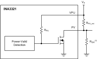
The PV pin allows for a 0-V output that indicates a power-invalid condition. An output equal to the pull-up supply voltage connected to the VPU pin indicates a power-valid condition, as shown in Figure 8-2. It is also possible to divide down the high power-valid pull-up voltage by adding a resistor to ground at the PV output, thus allowing this function to interface with lower-voltage circuitry, if needed.
