SBOS445C July 2008 – December 2015 INA333
PRODUCTION DATA.
- 1 Features
- 2 Applications
- 3 Description
- 4 Revision History
- 5 Pin Configuration and Functions
- 6 Specifications
- 7 Detailed Description
- 8 Application and Implementation
- 9 Power Supply Recommendations
- 10Layout
- 11Device and Documentation Support
- 12Mechanical, Packaging, and Orderable Information
Package Options
Mechanical Data (Package|Pins)
Thermal pad, mechanical data (Package|Pins)
- DRG|8
Orderable Information
1 Features
- Low Offset Voltage: 25 μV (Maximum), G ≥ 100
- Low Drift: 0.1 μV/°C, G ≥ 100
- Low Noise: 50 nV/√Hz, G ≥ 100
- High CMRR: 100 dB (Minimum), G ≥ 10
- Low Input Bias Current: 200 pA (Maximum)
- Supply Range: 1.8 V to 5.5 V
- Input Voltage: (V–) +0.1 V to (V+) –0.1 V
- Output Range: (V–) +0.05 V to (V+) –0.05 V
- Low Quiescent Current: 50 μA
- Operating Temperature: –40°C to +125°C
- RFI Filtered Inputs
- 8-Pin VSSOP and 8-Pin WSON Packages
2 Applications
- Bridge Amplifiers
- ECG Amplifiers
- Pressure Sensors
- Medical Instrumentation
- Portable Instrumentation
- Weigh Scales
- Thermocouple Amplifiers
- RTD Sensor Amplifiers
- Data Acquisition
3 Description
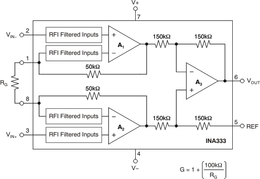
The INA333 device is a low-power, precision instrumentation amplifier offering excellent accuracy. The versatile 3-operational amplifier design, small size, and low power make it ideal for a wide range of portable applications.
A single external resistor sets any gain from 1 to 1000. The INA333 is designed to use an industry-standard gain equation: G = 1 + (100 kΩ / RG).
The INA333 device provides very low offset voltage (25 μV, G ≥ 100), excellent offset voltage drift
(0.1 μV/°C, G ≥ 100), and high common-mode rejection (100 dB at G ≥ 10). It operates with power supplies as low as 1.8 V (±0.9 V) and quiescent current is only 50 μA, making it ideal for battery-operated systems. Using autocalibration techniques to ensure excellent precision over the extended industrial temperature range, the INA333 device also offers exceptionally low noise density (50 nV/√Hz) that extends down to DC.
The INA333 device is available in both 8-pin VSSOP and WSON surface-mount packages and is specified over the TA = –40°C to +125°C temperature range.
Device Information(1)
| PART NUMBER | PACKAGE | BODY SIZE (NOM) |
|---|---|---|
| INA333 | VSSOP (8) | 3.00 mm × 3.00 mm |
| WSON (8) | 3.00 mm × 3.00 mm |
- For all available packages, see the orderable addendum at the end of the data sheet.
Simplified Schematic
