SBOSAD5D December   2022  – November 2024 INA351

PRODUCTION DATA  

  1.   1
  2. Features
  3. Applications
  4. Description
  5. Device Comparison Table
  6. Pin Configuration and Functions
  7. Specifications
    1. 6.1 Absolute Maximum Ratings
    2. 6.2 ESD Ratings
    3. 6.3 Recommended Operating Conditions
    4. 6.4 Thermal Information
    5. 6.5 Electrical Characteristics
    6. 6.6 Typical Characteristics
  8. Detailed Description
    1. 7.1 Overview
    2. 7.2 Functional Block Diagram
    3. 7.3 Feature Description
      1. 7.3.1 Gain-Setting
        1. 7.3.1.1 Gain Error and Drift
      2. 7.3.2 Input Common-Mode Voltage Range
      3. 7.3.3 EMI Rejection
      4. 7.3.4 Typical Specifications and Distributions
      5. 7.3.5 Electrical Overstress
    4. 7.4 Device Functional Modes
  9. Application and Implementation
    1. 8.1 Application Information
      1. 8.1.1 Reference Pin
      2. 8.1.2 Input Bias Current Return Path
    2. 8.2 Typical Applications
      1. 8.2.1 Resistive-Bridge Pressure Sensor
        1. 8.2.1.1 Design Requirements
        2. 8.2.1.2 Detailed Design Procedure
        3. 8.2.1.3 Application Curves
    3. 8.3 Power Supply Recommendations
    4. 8.4 Layout
      1. 8.4.1 Layout Guidelines
      2. 8.4.2 Layout Example
  10. Device and Documentation Support
    1. 9.1 Device Support
      1. 9.1.1 Development Support
        1. 9.1.1.1 PSpice® for TI
    2. 9.2 Documentation Support
      1. 9.2.1 Related Documentation
    3. 9.3 Receiving Notification of Documentation Updates
    4. 9.4 Support Resources
    5. 9.5 Trademarks
    6. 9.6 Electrostatic Discharge Caution
    7. 9.7 Glossary
  11. 10Revision History
  12. 11Mechanical, Packaging, and Orderable Information

Package Options

Mechanical Data (Package|Pins)
Thermal pad, mechanical data (Package|Pins)
Orderable Information

Application Curves

The following typical characteristic curve is for the circuit in Figure 8-4.
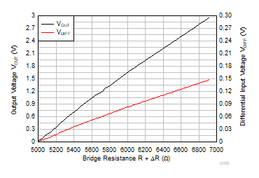
INA351 Input
                                                Differential Voltage, Output Voltage vs Bridge
                                                Resistance
Figure 8-6 Input Differential Voltage, Output Voltage vs Bridge Resistance