SLYS041A March 2020 – March 2021 INA381-Q1
PRODUCTION DATA
- 1 Features
- 2 Applications
- 3 Description
- 4 Revision History
- 5 Pin Configuration and Functions
- 6 Specifications
- 7 Detailed Description
- 8 Applications and Implementation
- 9 Power Supply Recommendations
- 10Layout
- 11Device and Documentation Support
- 12Mechanical, Packaging, and Orderable Information
Package Options
Mechanical Data (Package|Pins)
- DGS|10
Thermal pad, mechanical data (Package|Pins)
Orderable Information
8.1.4 Input Filtering
If the INA381-Q1 output is connected to a high-impedance input, the device output is the best location to filter, using a simple RC network from VOUT to GND. Filtering at the output attenuates high-frequency disturbances in the common-mode voltage, differential input signal, and INA381-Q1 power-supply voltage. If filtering at the output is not possible, or if only the differential input signal needs filtering, a filter can be applied at the input pins of the device.
External filtering helps reduce the amount of noise that reaches the comparator, and thereby reduces the likelihood of a false alert. The tradeoff to adding this noise filter is that the alert response time is increased because both the input signal and noise are filtered. Figure 8-4 shows the implementation of an input filter for the device.
 Figure 8-4 Input Filter
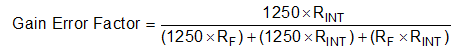
The addition of external series resistance creates an additional error in the measurement; therefore, the value of these series resistors must be kept to 10 Ω (or less, if possible) to reduce impact to accuracy. As shown in Figure 8-4, the internal bias network present at the input pins creates a mismatch in input bias currents when a differential voltage is applied between the input pins. If additional external series filter resistors are added to the circuit, the mismatch in bias currents results in a mismatch of voltage drops across the filter resistors. This mismatch creates a differential error voltage that subtracts from the voltage developed across the shunt resistor. This error results in a voltage at the device input pins that is different than the voltage developed across the shunt resistor. Without the additional series resistance, the mismatch in input bias currents has negligible effect on device operation. Equation 2 is used to calculate the gain error factor that is used with Equation 3 to calculate the percentage gain error when using external filter resistors.
Equation 2 shows that the amount of variance in the differential voltage present at the device input relative to the voltage developed at the shunt resistor is based both on the external series resistance (RF) value as well as internal input resistor RINT. The reduction of the shunt voltage reaching the device input pins appears as a gain error when comparing the output voltage relative to the voltage across the shunt resistor. Use Equation 2 to calculate the expected deviation from the shunt voltage to what is measured at the device input pins:
where:
- RINT is the internal input resistor
- RF is the external series resistance
The adjustment factor from Equation 2 including the device internal input resistance shown in Table 8-3 varies with each gain version. Table 8-4 lists each individual device gain error factor.
| PRODUCT | GAIN | RINT (kΩ) |
|---|---|---|
| INA381A1-Q1 | 20 | 25 |
| INA381A2-Q1 | 50 | 10 |
| INA381A3-Q1 | 100 | 5 |
| INA381A4-Q1 | 200 | 2.5 |
| PRODUCT | SIMPLIFIED GAIN ERROR FACTOR |
|---|---|
| INA381A1-Q1 | 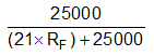 |
| INA381A2-Q1 | 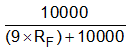 |
| INA381A3-Q1 |  |
| INA381A4-Q1 | 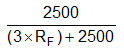 |
Use Equation 3 to then calculate the gain error that can be expected from the addition of the external series resistors:

For example, using an INA381A2-Q1 and the corresponding gain error equation from Table 8-4, a series resistance of 10 Ω results in a gain error factor of 0.991. The corresponding gain error is then calculated using Equation 3, resulting in an additional gain error of approximately 0.89% solely because of the external 10-Ω series resistors.