SBOSAI9B December 2023 – March 2024 INA500
PRODMIX
- 1
- 1 Features
- 2 Applications
- 3 Description
- 4 Device Comparison Table
- 5 Pin Configuration and Functions
- 6 Specifications
- 7 Detailed Description
- 8 Application and Implementation
- 9 Device and Documentation Support
- 10Revision History
- 11Mechanical, Packaging, and Orderable Information
Package Options
Refer to the PDF data sheet for device specific package drawings
Mechanical Data (Package|Pins)
- DBV|6
- DCK|6
Thermal pad, mechanical data (Package|Pins)
Orderable Information
7.3.2 Input Common-Mode Voltage Range
The INA500 difference-amplifier rejects the input common mode. The rejection capability is based on the matching of the internal resistors. The input voltage range of the INA500 is primarily dictated by the signal swing at the op-amp inputs. The INA500 input common-mode voltage range can extend well beyond the supply rails and is a major function of the gain configuration. To maximize performance, it is critical to keep the op-amp inside the INA500 within the linear range for a given combination of gain, reference voltage, and input common-mode voltage for a particular input differential voltage and output swing.
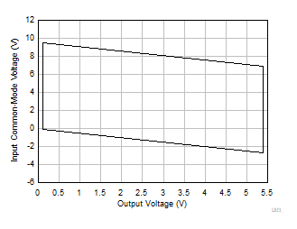
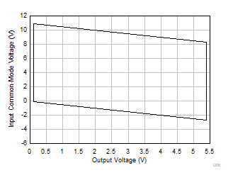
Input common-mode voltage (VCM) vs output voltage graphs (VOUT) in this section outlines the linear performance region of the INA500 for a particular combination of gain and reference voltage values. A good common-mode rejection can be expected when operating with in the limits of the VCM versus VOUT graph. The common-mode range for the INA500 in equation form is outlined in the Electrical Characteristics for each gain. The most common operating conditions are outlined graphically in the Typical Characteristics section. Figure 7-79 shows the region of operation where a minimum of 75dB CMRR can be achieved. This is referred as the high CMRR region. Figure 7-80 has much wider region of operation with a lower CMRR of 62dB minimum. This is because the input signal crosses over the transition region of the input pairs to achieve rail-to-rail operation.

| V+ = 5.5V | V– = 0V | G = 1 | VREF = 0V |

| V+ = 5.5V | V– = 0V | G = 1 | VREF = 0V |