SBOSAB6A July   2023  – December 2023 INA780A , INA780B

PRODMIX  

  1.   1
  2. Features
  3. Applications
  4. Description
  5. Pin Configuration and Functions
  6. Specifications
    1. 5.1 Absolute Maximum Ratings
    2. 5.2 ESD Ratings
    3. 5.3 Recommended Operating Conditions
    4. 5.4 Thermal Information
    5. 5.5 Electrical Characteristics
    6. 5.6 Timing Requirements (I2C)
    7. 5.7 Timing Diagram
    8. 5.8 Typical Characteristics
  7. Detailed Description
    1. 6.1 Overview
    2. 6.2 Functional Block Diagram
    3. 6.3 Feature Description
      1. 6.3.1 Integrated Shunt Resistor
      2. 6.3.2 Safe Operating Area
      3. 6.3.3 Versatile High Voltage Measurement Capability
      4. 6.3.4 Internal Measurement and Calculation Engine
      5. 6.3.5 High-Precision Delta-Sigma ADC
        1. 6.3.5.1 Low Latency Digital Filter
        2. 6.3.5.2 Flexible Conversion Times and Averaging
      6. 6.3.6 Integrated Precision Oscillator
      7. 6.3.7 Multi-Alert Monitoring and Fault Detection
    4. 6.4 Device Functional Modes
      1. 6.4.1 Shutdown Mode
      2. 6.4.2 Power-On Reset
    5. 6.5 Programming
      1. 6.5.1 I2C Serial Interface
        1. 6.5.1.1 Writing to and Reading Through the I2C Serial Interface
        2. 6.5.1.2 High-Speed I2C Mode
        3. 6.5.1.3 SMBus Alert Response
  8. Application and Implementation
    1. 7.1 Application Information
      1. 7.1.1 Device Measurement Range and Resolution
      2. 7.1.2 ADC Output Data Rate and Noise Performance
    2. 7.2 Typical Application
      1. 7.2.1 Design Requirements
      2. 7.2.2 Detailed Design Procedure
        1. 7.2.2.1 Configure the Device
        2. 7.2.2.2 Set Desired Fault Thresholds
        3. 7.2.2.3 Calculate Returned Values
      3. 7.2.3 Application Curves
    3. 7.3 Power Supply Recommendations
    4. 7.4 Layout
      1. 7.4.1 Layout Guidelines
      2. 7.4.2 Layout Example
    5. 7.5 Register Maps
      1. 7.5.1 INA780x Registers
  9. Device and Documentation Support
    1. 8.1 Receiving Notification of Documentation Updates
    2. 8.2 Support Resources
    3. 8.3 Trademarks
    4. 8.4 Electrostatic Discharge Caution
    5. 8.5 Glossary
  10. Revision History
  11. 10Mechanical, Packaging, and Orderable Information

Package Options

Mechanical Data (Package|Pins)
Thermal pad, mechanical data (Package|Pins)
Orderable Information

Typical Characteristics

at TA = 25°C, VVS = 3.3 V, VCM = 48 V, VSENSE = 0, and VVBUS = 48 V (unless otherwise noted)

GUID-20231218-SS0I-VBCH-SKDS-BZ9XR0CQD6LZ-low.svg
Figure 5-2 Shunt Input Offset Current Production Distribution (B Devices)
GUID-20231218-SS0I-PSB1-4FLJ-WQK5XDQSG3FS-low.svg
Figure 5-4 Common-Mode Rejection Ratio Production Distribution
GUID-20231218-SS0I-9GKZ-CVLT-8CH4P47C5JJF-low.svg
VCM = 24 V
Figure 5-6 Current Gain Error Production Distribution
GUID-20201109-CA0I-5BWC-XQS8-7NBH2VMQP0CD-low.svg
Figure 5-8 Current Gain Error vs Common-Mode Voltage
GUID-20231116-SS0I-FQMS-VN0F-KS4CWZZ1BLVC-low.svg
VVBUS = 20 mV
Figure 5-10 Bus Input Offset Voltage vs Temperature
GUID-20231116-SS0I-LNDC-HKJH-F0TS4PTR4GHX-low.svg
Figure 5-12 Bus Input Gain Error vs Temperature
GUID-E26E67F0-4417-4A9F-96B7-247A9E37A104-low.svg
Figure 5-14 Input Bias Current vs Temperature
GUID-DBDA86E1-B489-4CDD-AC16-739B555CF581-low.svg
Figure 5-16 Active IQ vs Temperature
GUID-7A583524-872B-4240-9B52-8CD6C6688AA3-low.svg
Figure 5-18 Shutdown IQ vs Supply Voltage
GUID-42C47846-361C-4853-925A-DE90393568E2-low.gif
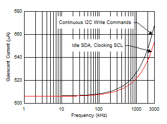
Figure 5-20 Active IQ vs Clock Frequency
GUID-05B96C14-9B24-44FE-995E-C833ED5B0FA4-low.svg
Figure 5-22 Internal Clock Frequency vs Power Supply
GUID-20231116-SS0I-PJJP-HZCW-L0Z72GBSZKPG-low.svg
Figure 5-3 Input Offset Current vs Temperature
GUID-20231116-SS0I-HH9F-3CFQ-JMKDCSLHH5KK-low.svg
Figure 5-5 Current Common-Mode Rejection Ratio vs Temperature
GUID-20231116-SS0I-V0FS-F64G-TFDNGKTSHJCR-low.svg
VCM = 24 V
Figure 5-7 Current Gain Error vs Temperature
GUID-20231218-SS0I-CDNV-KVZP-QKZJRCZ39TSF-low.svg
VVBUS = 20 mV
Figure 5-9 Bus Input Offset Voltage Production Distribution
GUID-20231218-SS0I-B0T6-LXJ7-D56G4W4NL7S5-low.svg
Figure 5-11 Bus Input Gain Error Production Distribution
GUID-686701FD-3CED-479C-9107-0B805DE8B511-low.svg
Figure 5-13 Input Bias Current (IB+ or IB–) vs Common-Mode Voltage
GUID-92E139E8-B1E2-45ED-B766-65C20EFF7DC6-low.svg
Figure 5-15 Input Bias Current vs Temperature, Shutdown
GUID-8ECEF12C-8C7F-4BAF-9791-5E4BAC383821-low.svg
Figure 5-17 Active IQ vs Supply Voltage
GUID-20231116-SS0I-TDVP-5NJV-XG0QDCLLSKRP-low.svg
Figure 5-19 Shutdown IQ vs Temperature
GUID-FA1AF79A-A76B-46DF-B67E-662CA0711177-low.gif
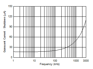
Figure 5-21 Shutdown IQ vs Clock Frequency
GUID-A9167CC2-9579-4E2C-9FB1-F7267F6A4B61-low.svg
Figure 5-23 Internal Clock Frequency vs Temperature