SBOS959D December 2018 – April 2022 INA819
PRODUCTION DATA
- 1 Features
- 2 Applications
- 3 Description
- 4 Revision History
- 5 Device Comparison Table
- 6 Pin Configuration and Functions
- 7 Specifications
- 8 Detailed Description
- 9 Application and Implementation
- 10Power Supply Recommendations
- 11Layout
- 12Device and Documentation Support
- 13Mechanical, Packaging, and Orderable Information
Package Options
Mechanical Data (Package|Pins)
Thermal pad, mechanical data (Package|Pins)
- DRG|8
Orderable Information
8.3.1 Setting the Gain
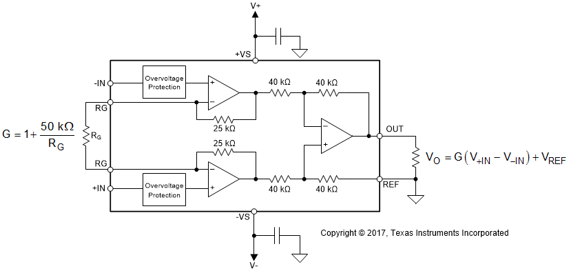
Figure 8-1 shows that the gain of the INA819 is set by a single external resistor (RG) connected between the RG pins (pins 1 and 8).
 Figure 8-1 Simplified Diagram of the INA819 With Gain and Output Equations
The value of RG is selected according to Equation 1:

Table 8-1 lists several commonly used gains and resistor values. The 50-kΩ term in Equation 1 is a result of the sum of the two internal 25-kΩ feedback resistors. These on-chip resistors are laser-trimmed to accurate absolute values. The accuracy and temperature coefficients of these resistors are included in the gain accuracy and drift specifications of the INA819. As shown in Figure 8-1 and explained in more details in Section 11, make sure to connect low-ESR, 0.1-µF ceramic bypass capacitors between each supply pin and ground that are placed as close to the device as possible.
| DESIRED GAIN | RG (Ω) | NEAREST 1% RG (Ω) |
|---|---|---|
| 1 | NC | NC |
| 2 | 50 k | 49.9 k |
| 5 | 12.5 k | 12.4 k |
| 10 | 5.556 k | 5.49 k |
| 20 | 2.632 k | 2.61 k |
| 50 | 1.02 k | 1.02 k |
| 100 | 505.1 | 511 |
| 200 | 251.3 | 249 |
| 500 | 100.2 | 100 |
| 1000 | 50.05 | 49.9 |