SBOS959D December   2018  – April 2022 INA819

PRODUCTION DATA  

  1. Features
  2. Applications
  3. Description
  4. Revision History
  5. Device Comparison Table
  6. Pin Configuration and Functions
  7. Specifications
    1. 7.1 Absolute Maximum Ratings
    2. 7.2 ESD Ratings
    3. 7.3 Recommended Operating Conditions
    4. 7.4 Thermal Information
    5. 7.5 Electrical Characteristics
    6. 7.6 Typical Characteristics
  8. Detailed Description
    1. 8.1 Overview
    2. 8.2 Functional Block Diagram
    3. 8.3 Feature Description
      1. 8.3.1 Setting the Gain
        1. 8.3.1.1 Gain Drift
      2. 8.3.2 EMI Rejection
      3. 8.3.3 Input Common-Mode Range
      4. 8.3.4 Input Protection
      5. 8.3.5 Operating Voltage
      6. 8.3.6 Error Sources
    4. 8.4 Device Functional Modes
  9. Application and Implementation
    1. 9.1 Application Information
      1. 9.1.1 Reference Pin
      2. 9.1.2 Input Bias Current Return Path
    2. 9.2 Typical Applications
      1. 9.2.1 Three-Pin Programmable Logic Controller (PLC)
        1. 9.2.1.1 Design Requirements
        2. 9.2.1.2 Detailed Design Procedure
        3. 9.2.1.3 Application Curves
      2. 9.2.2 Resistance Temperature Detector Interface
  10. 10Power Supply Recommendations
  11. 11Layout
    1. 11.1 Layout Guidelines
    2. 11.2 Layout Example
  12. 12Device and Documentation Support
    1. 12.1 Device Support
      1. 12.1.1 Development Support
        1. 12.1.1.1 PSpice® for TI
        2. 12.1.1.2 TINA-TI™ Simulation Software (Free Download)
    2. 12.2 Documentation Support
      1. 12.2.1 Related Documentation
    3. 12.3 Receiving Notification of Documentation Updates
    4. 12.4 Support Resources
    5. 12.5 Trademarks
    6. 12.6 Electrostatic Discharge Caution
    7. 12.7 Glossary
  13. 13Mechanical, Packaging, and Orderable Information

Package Options

Mechanical Data (Package|Pins)
Thermal pad, mechanical data (Package|Pins)
Orderable Information

Typical Characteristics

at TA = 25°C, VS = ±15 V, RL = 10 kΩ, VREF = 0 V, and G = 1 (unless otherwise noted)

Table 7-1 Table of Graphs
DESCRIPTION FIGURE
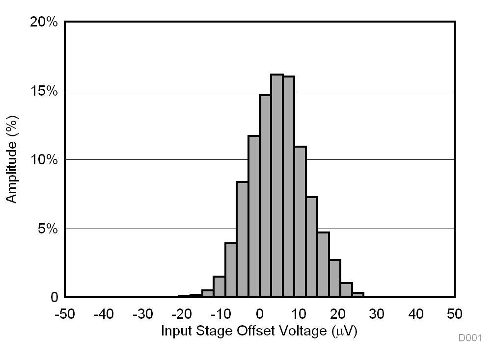
Typical Distribution of Input Stage Offset Voltage Figure 7-1
Typical Distribution of Input Stage Offset Voltage Drift Figure 7-2
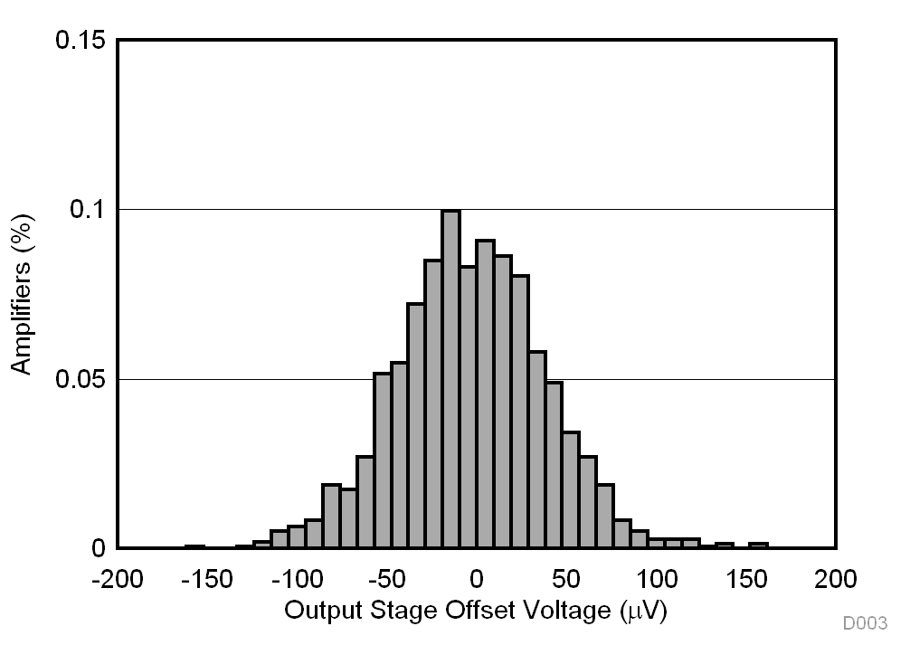
Typical Distribution of Output Stage Offset Voltage Figure 7-3
Typical Distribution of Output Stage Offset Voltage Drift Figure 7-4
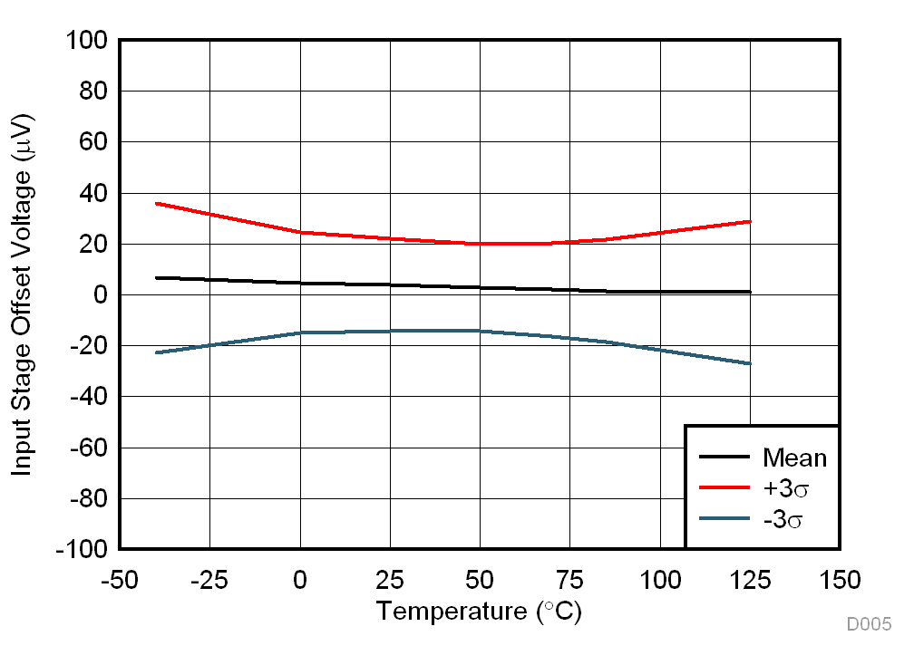
Input Stage Offset Voltage vs Temperature Figure 7-5
Output Stage Offset Voltage vs Temperature Figure 7-6
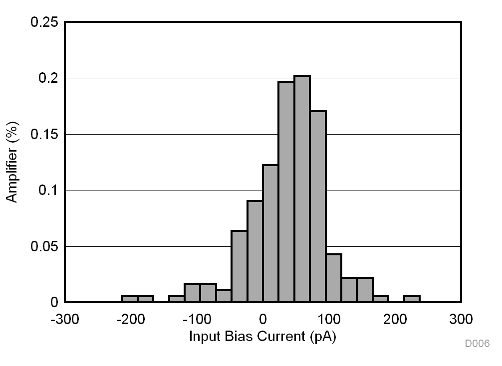
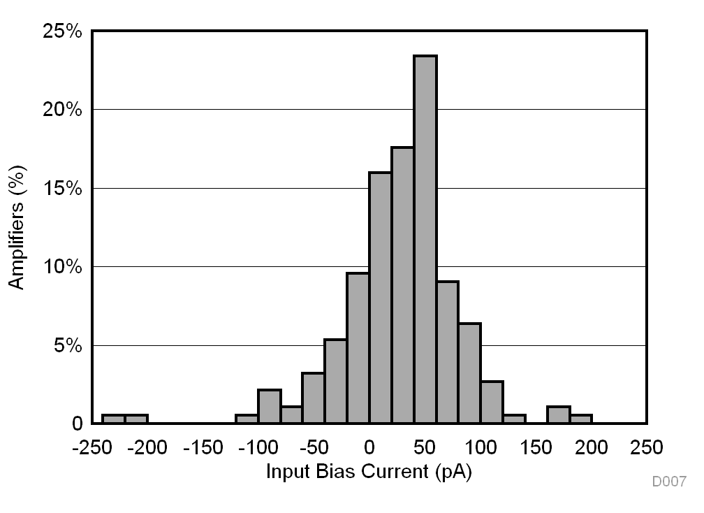
Typical Distribution of Input Bias Current, TA = 25°C Figure 7-7
Typical Distribution of Input Bias Current, TA = 90°C Figure 7-8
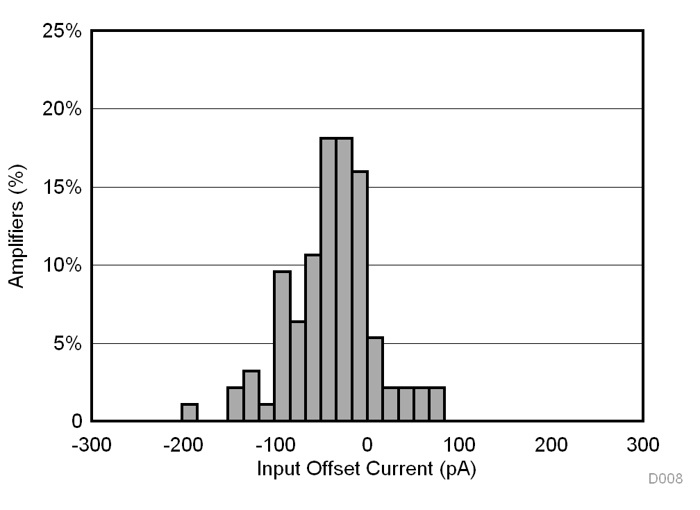
Typical Distribution of Input Offset Current Figure 7-9
Input Bias Current vs Temperature Figure 7-10
Input Offset Current vs Temperature Figure 7-11
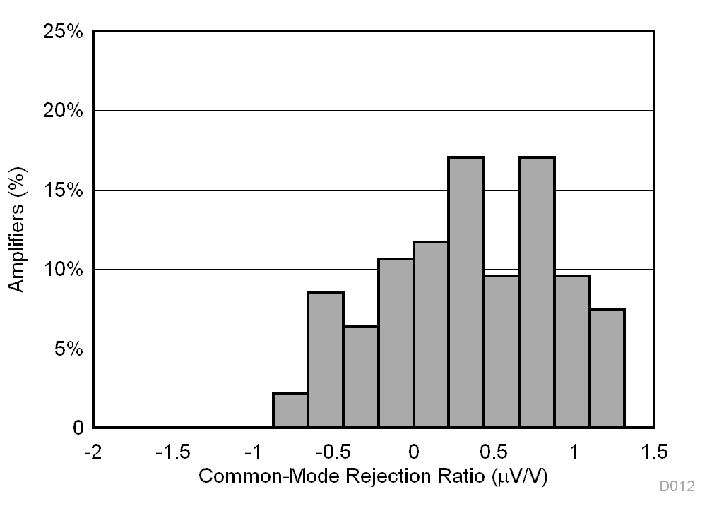
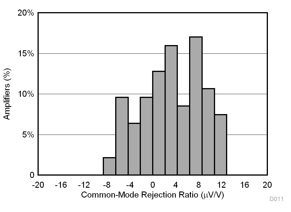
Typical CMRR Distribution, G = 1 Figure 7-12
Typical CMRR Distribution, G = 10 Figure 7-13
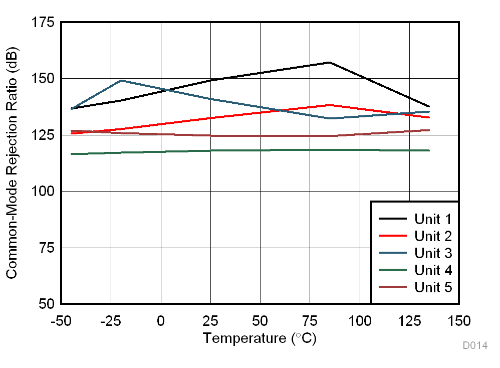
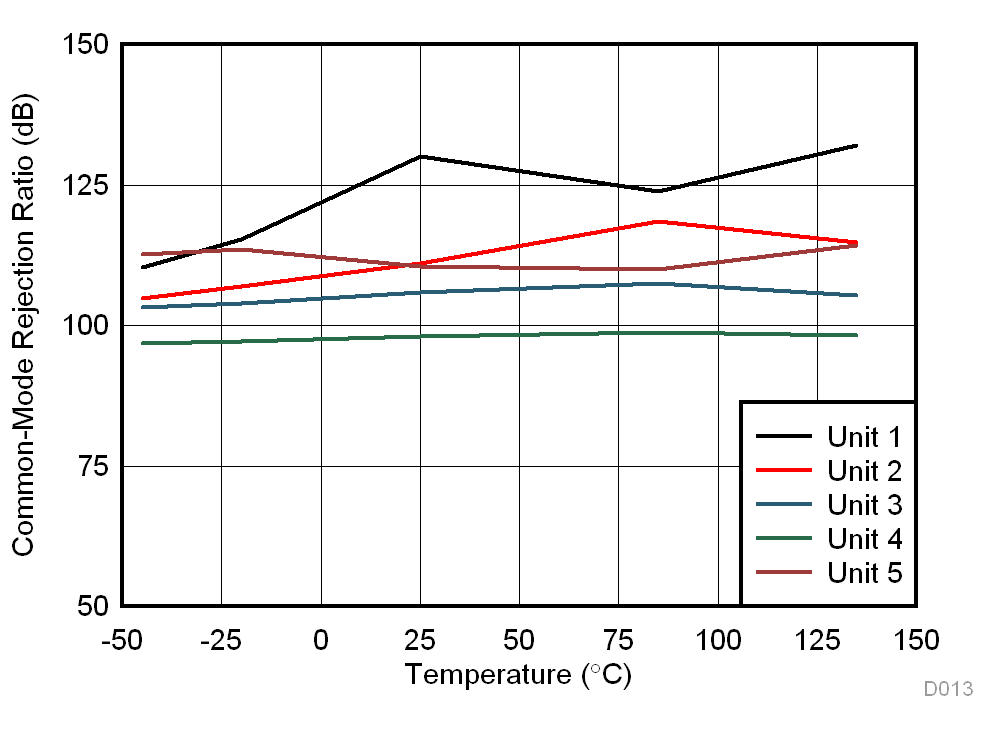
CMRR vs Temperature, G = 1 Figure 7-14
CMRR vs Temperature, G = 10 Figure 7-15
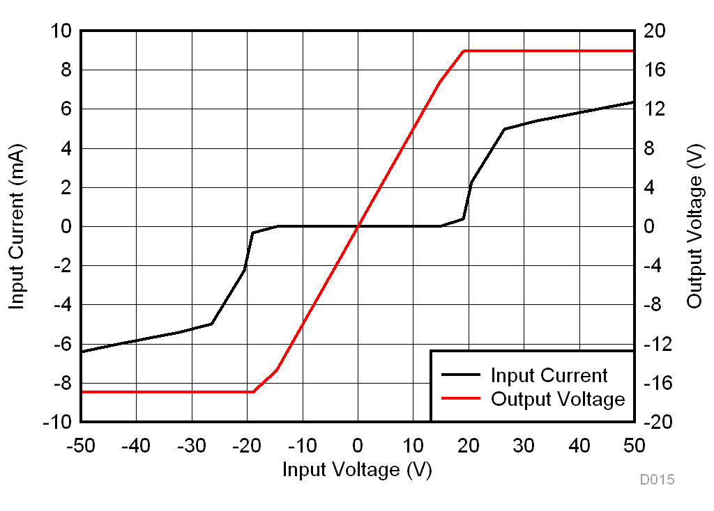
Input Current vs Input Overvoltage Figure 7-16
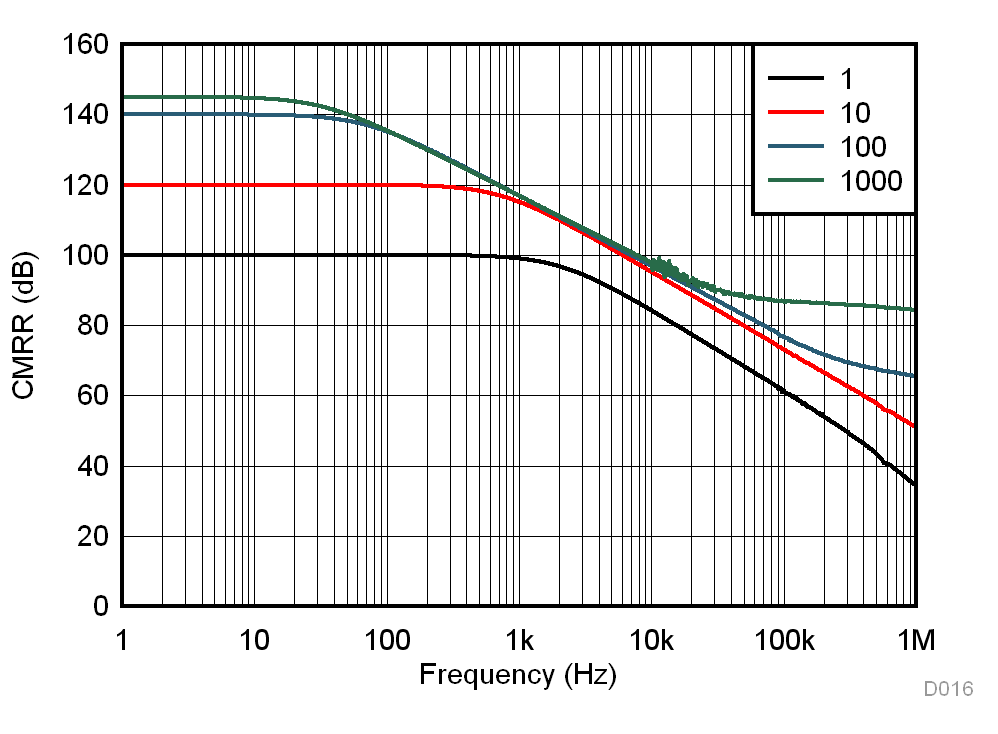
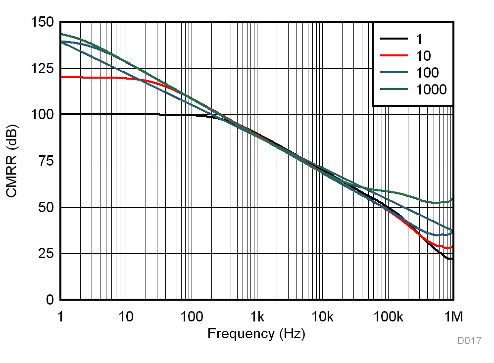
CMRR vs Frequency (RTI) Figure 7-17
CMRR vs Frequency (RTI, 1-kΩ source imbalance) Figure 7-18
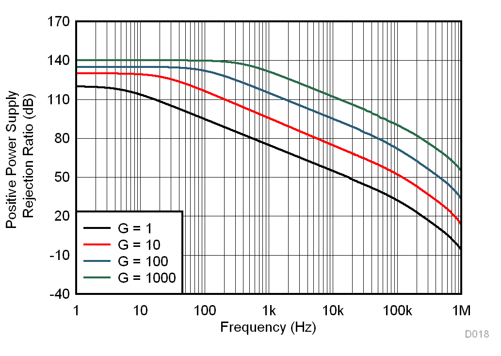
Positive PSRR vs Frequency (RTI) Figure 7-19
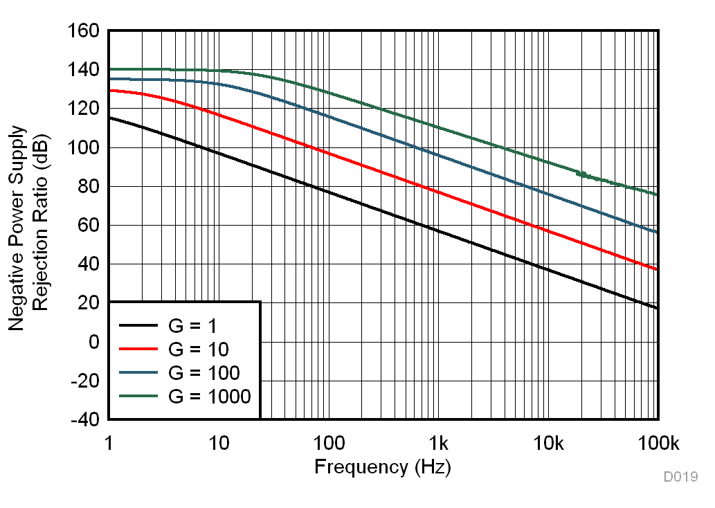
Negative PSRR vs Frequency (RTI) Figure 7-20
Gain vs Frequency Figure 7-21
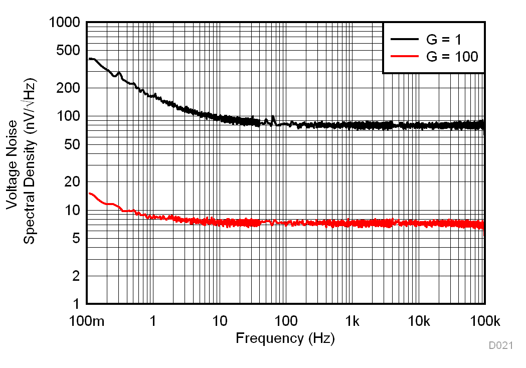
Voltage Noise Spectral Density vs Frequency (RTI) Figure 7-22
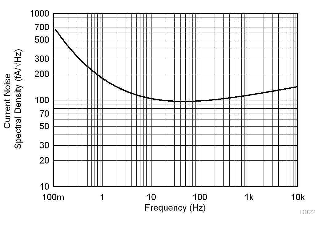
Current Noise Spectral Density vs Frequency (RTI) Figure 7-23
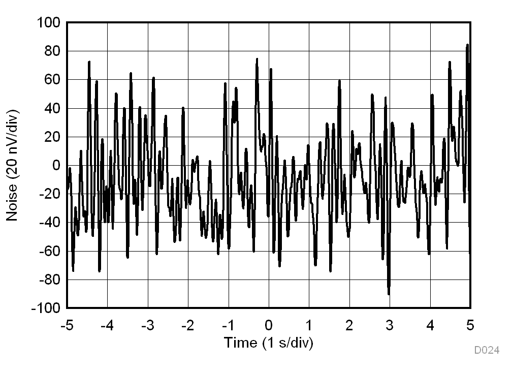
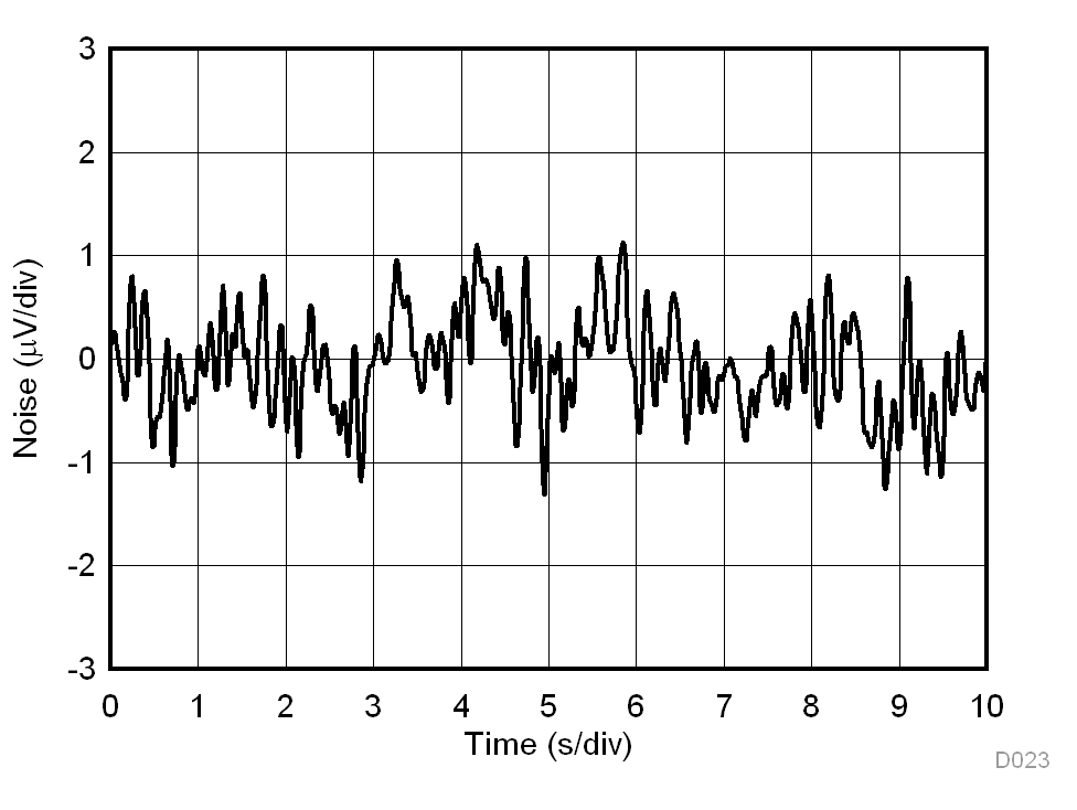
0.1-Hz to 10-Hz RTI Voltage Noise, G = 1 Figure 7-24
0.1-Hz to 10-Hz RTI Voltage Noise, G = 1000 Figure 7-25
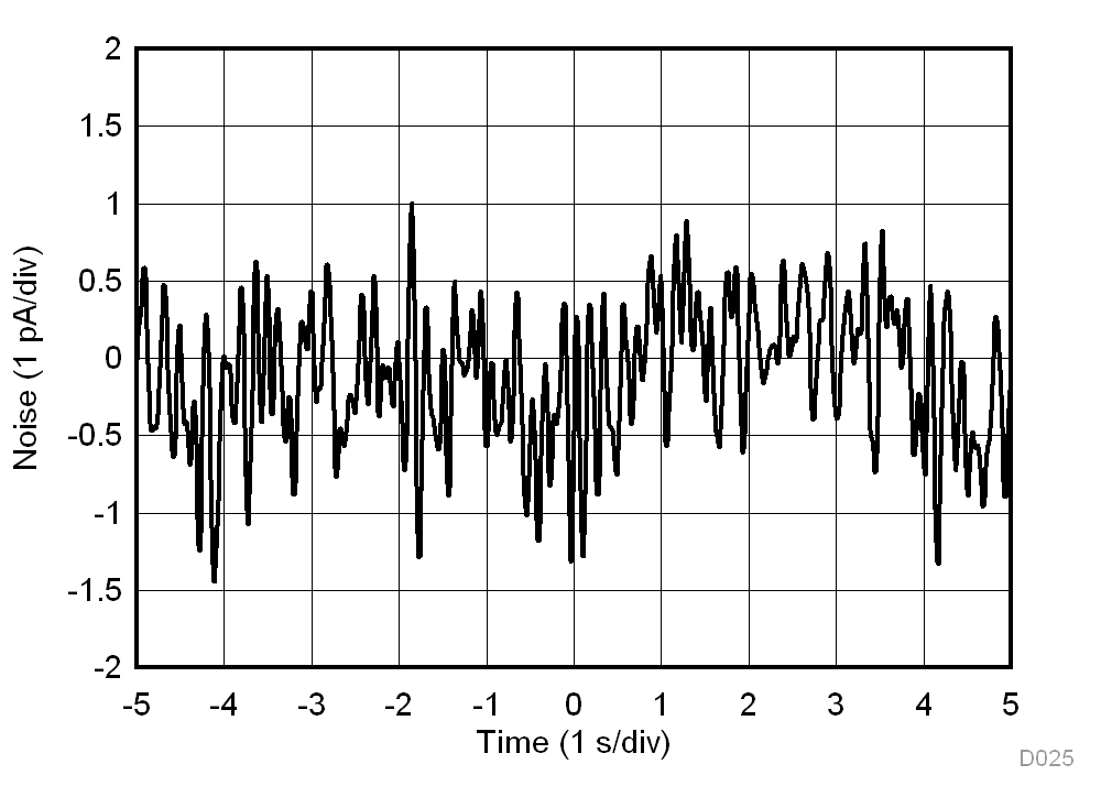
0.1-Hz to 10-Hz RTI Current Noise Figure 7-26
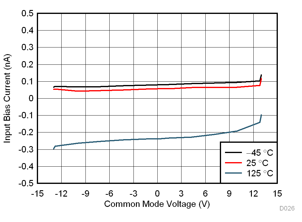
Input Bias Current vs Common-Mode Voltage Figure 7-27
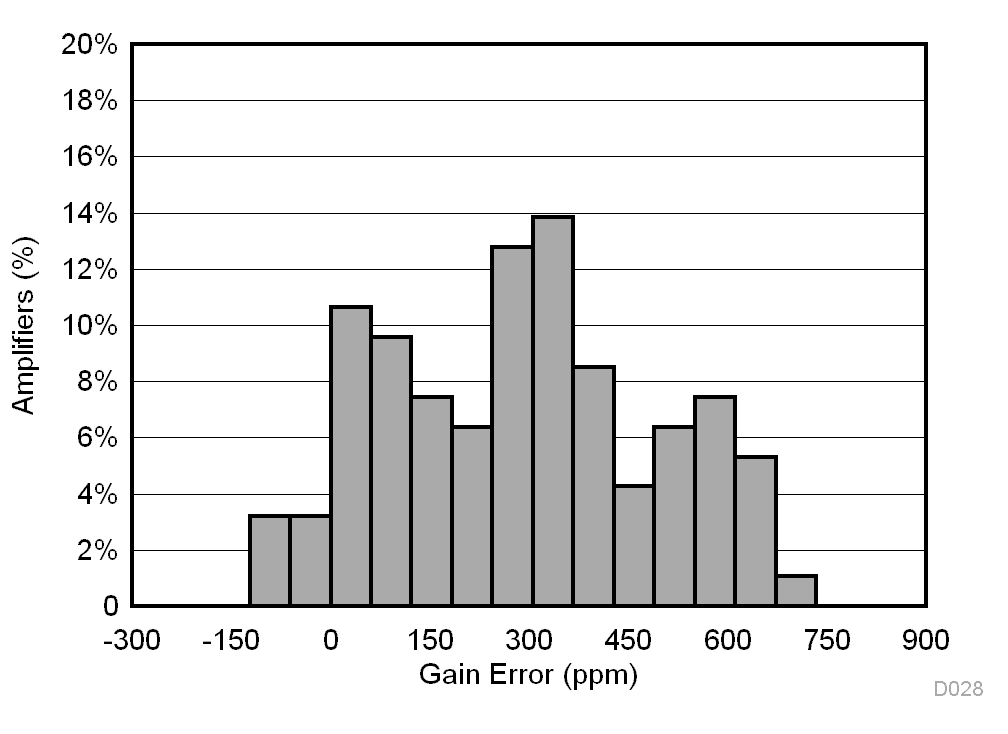
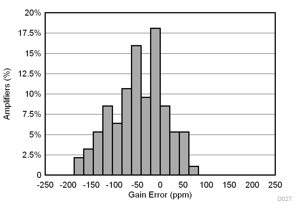
Typical Distribution of Gain Error, G = 1 Figure 7-28
Typical Distribution of Gain Error, G = 10 Figure 7-29
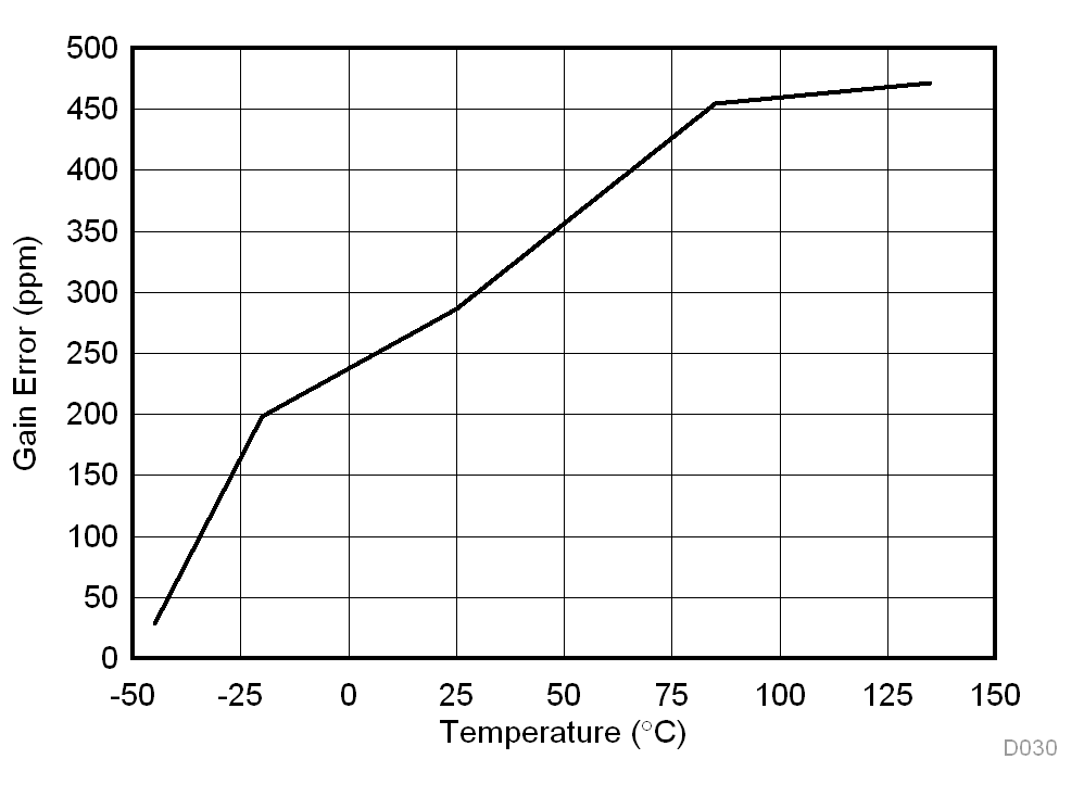
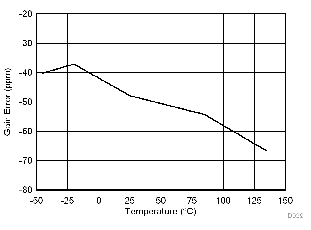
Gain Error vs Temperature, G = 1 Figure 7-30
Gain Error vs Temperature, G = 10 Figure 7-31
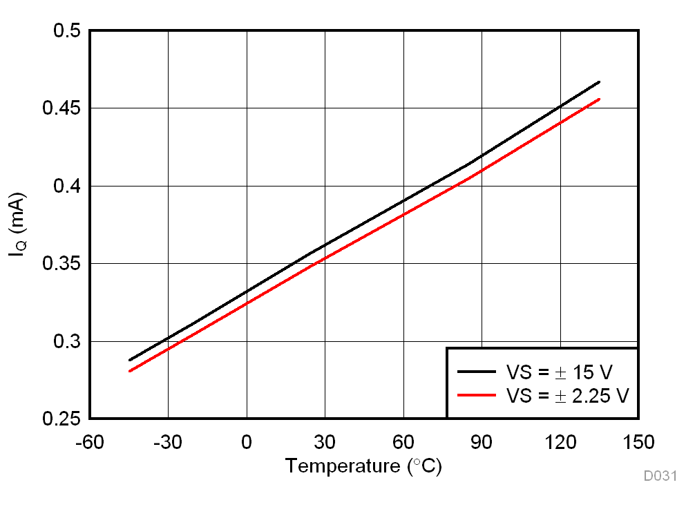
Supply Current vs Temperature Figure 7-32
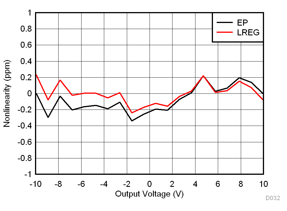
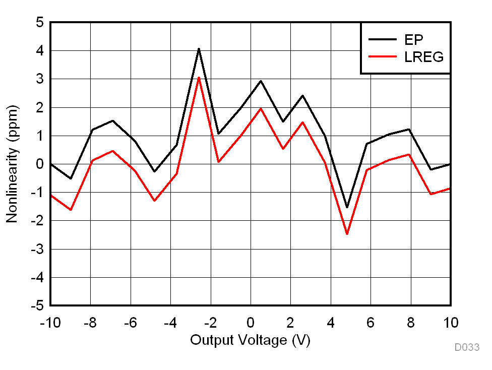
Gain Nonlinearity, G = 1 Figure 7-33
Gain Nonlinearity, G = 10 Figure 7-34
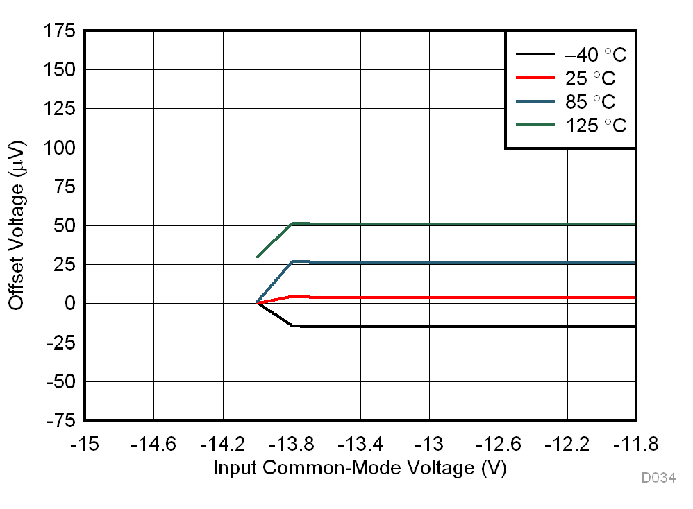
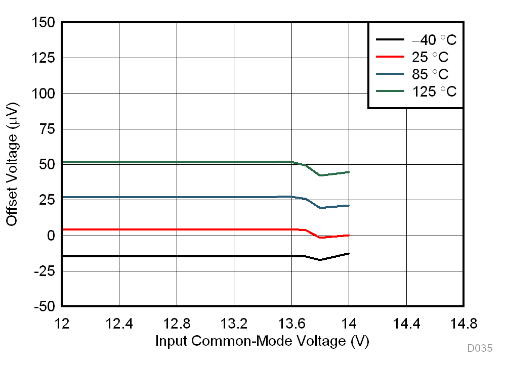
Offset Voltage vs Negative Common-Mode Voltage Figure 7-35
Offset Voltage vs Positive Common-Mode Voltage Figure 7-36
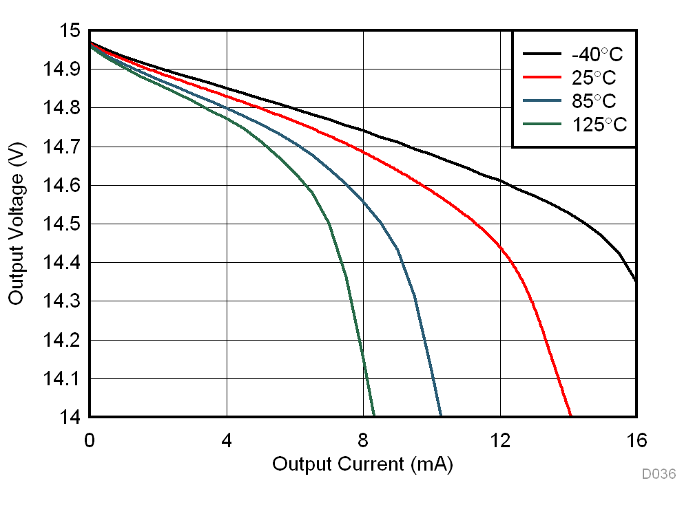
Positive Output Voltage Swing vs Output Current Figure 7-37
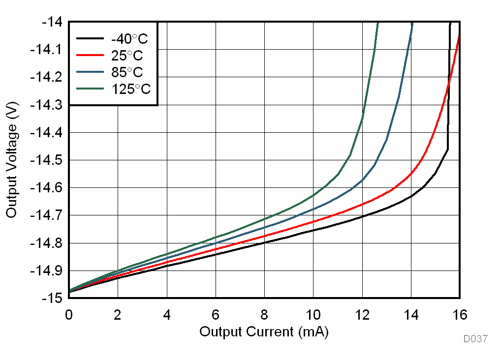
Negative Output Voltage Swing vs Output Current Figure 7-38
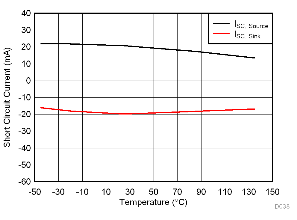
Short Circuit Current vs Temperature Figure 7-39
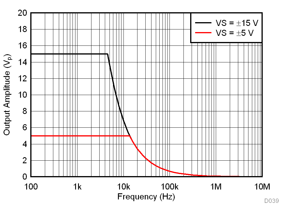
Large-Signal Frequency Response Figure 7-40
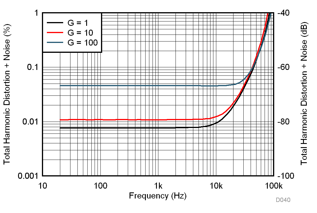
THD+N vs Frequency Figure 7-41
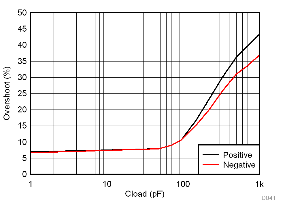
Overshoot vs Capacitive Loads Figure 7-42
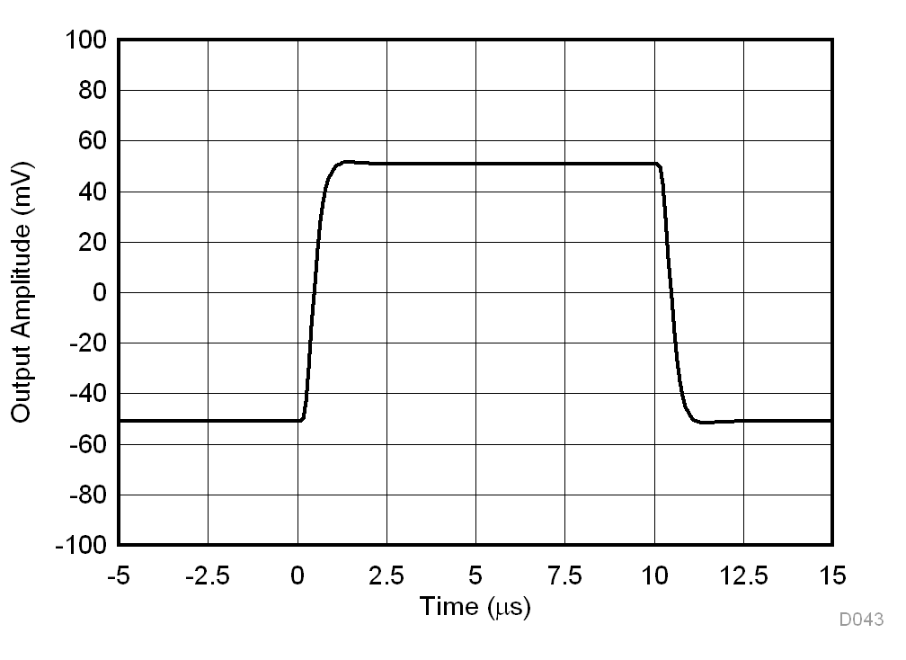
Small-Signal Response, G = 1 Figure 7-43
Small-Signal Response, G = 10 Figure 7-44
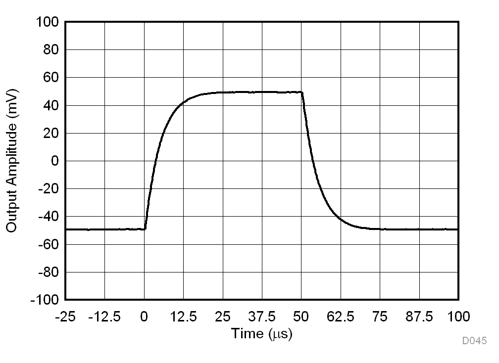
Small-Signal Response, G = 100 Figure 7-45
Small-Signal Response, G = 1000 Figure 7-46
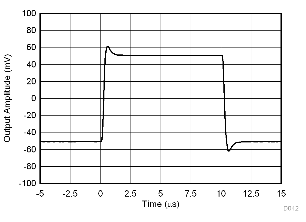
Large Signal Step Response Figure 7-47
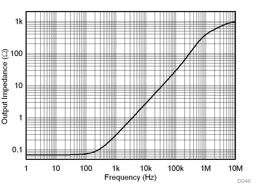
Closed-Loop Output Impedance Figure 7-48
Differential-Mode EMI Rejection Ratio Figure 7-49
Common-Mode EMI Rejection Ratio Figure 7-50
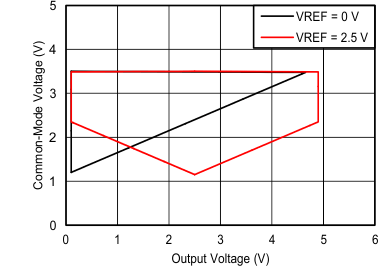
Input Common-Mode Voltage vs Output Voltage, G = 1, VS = 5 V Figure 7-51
Input Common-Mode Voltage vs Output Voltage, G = 100, VS = 5 V Figure 7-52
Input Common-Mode Voltage vs Output Voltage, VS =±5 V Figure 7-53
Input Common-Mode Voltage vs Output Voltage, VS =±15 V Figure 7-54
GUID-DEBD015B-920D-4183-9B02-E92ECCCF0B13-low.gif
N = 1555 Mean = 4.71 µV Std. Dev. = 7.12 µV
Figure 7-1 Typical Distribution of Input Stage Offset Voltage
GUID-0E0C6739-AB37-42C5-A79D-D80DC71ED980-low.gif
N = 1555 Mean = –3.18 µV Std. Dev. = 41.26 µV
Figure 7-3 Typical Distribution of Output Stage Offset Voltage
GUID-41E5EB80-2544-46CD-B4D3-D97E5B0B2131-low.gif
45 units, 1 wafer lot
Figure 7-5 Input Stage Offset Voltage vs Temperature
GUID-CA17CDD9-DF78-410B-9002-91CF4CAD19C8-low.gif
N = 94 Mean = 37.13 pA Std. Dev. = 57.65 pA
TA = 25°C
Figure 7-7 Typical Distribution of Input Bias Current
GUID-06BE8E93-965B-4731-8F40-EB5548D2CC39-low.gif
N = 94 Mean = –38.82 pA Std. Dev. = 47.24 pA
Figure 7-9 Typical Distribution of Input Offset Current
N = 94 G = 1
 
Figure 7-11 Input Offset Current vs Temperature
GUID-71B4AEDD-FFAD-4619-B763-4255A7400E25-low.gif
N = 94 Mean = 0.34 µV/V Std. Dev. = 0.54 µV/V
G = 10
Figure 7-13 Typical CMRR Distribution
GUID-78FC6929-D479-4D05-AABE-D9E87A5D03C4-low.gif
5 typical units G = 10
Figure 7-15 CMRR vs Temperature
GUID-B6BA954C-19CE-480F-A325-7C2786F44180-low.gif
 
Figure 7-17 CMRR vs Frequency (RTI)
GUID-B4185420-3939-4F18-81E0-8FDEF2406499-low.gif
 
Figure 7-19 Positive PSRR vs Frequency (RTI)
GUID-66C9FFA2-BFED-4A11-AFC7-77D9E8136E6C-low.gifFigure 7-21 Gain vs Frequency
GUID-A7E257EA-AB67-4BC4-807B-B2A3B62E00A3-low.gif
 
Figure 7-23 Current Noise Spectral Density vs Frequency (RTI)
GUID-F242931C-9B06-465D-AA03-9AAA20B23EAC-low.gif
G = 1000
Figure 7-25 0.1-Hz to 10-Hz RTI Voltage Noise
GUID-EDEE20EC-EA0B-4933-8CBE-EC3D489345E5-low.gif
VS = ±15 V
 
Figure 7-27 Input Bias Current vs Common-Mode Voltage
GUID-6FFB17E6-68AA-4CC9-AC21-68E8A9AD4343-low.gif
N = 94 Mean = 286 ppm Std. Dev. = 204 ppm
G = 10
Figure 7-29 Typical Distribution of Gain Error,
G = 10
GUID-187B77A6-6981-4293-A7F0-D971D394E43B-low.gif
G = 10
Figure 7-31 Gain Error vs Temperature
GUID-D23B5D4A-BF60-4F02-9822-B913E2C580D7-low.gif
G = 1
Figure 7-33 Gain Nonlinearity
GUID-898D9A8E-21C5-4DBD-A4E9-5C16A5C8351B-low.gif
 
Figure 7-35 Offset Voltage vs Negative Common-Mode Voltage
GUID-634E23A7-8852-4AB7-B7FD-8154EF190935-low.gif
 
Figure 7-37 Positive Output Voltage Swing vs Output Current
GUID-F910A8C4-3AD4-41B1-89D9-B3B81FD23424-low.gif
 
Figure 7-39 Short Circuit Current vs Temperature
GUID-18681AAC-3B00-4E24-B7B0-CB4591770DCF-low.gif
500-kHz measurement bandwidth
1-VRMS output voltage 100-kΩ load
Figure 7-41 THD+N vs Frequency
GUID-C0DE3388-F79A-4722-BA98-7F6BF003C796-low.gif
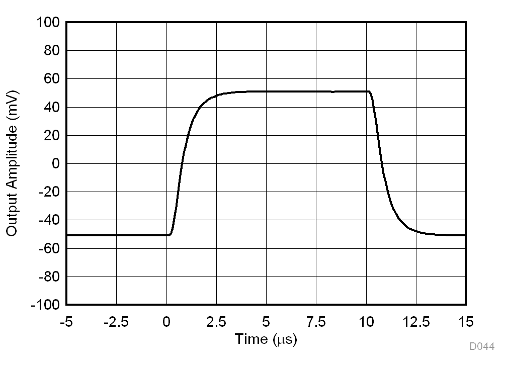
G = 1 RL = 10 kΩ CL = 100 pF
Figure 7-43 Small-Signal Response
GUID-1CD9A39D-3B89-4602-B649-9524FA820B13-low.gif
G = 100 RL = 10 kΩ CL = 100 pF
Figure 7-45 Small-Signal Response
GUID-8EC6D501-A9EB-4E4F-B0AD-7590627F2CC3-low.gif
 
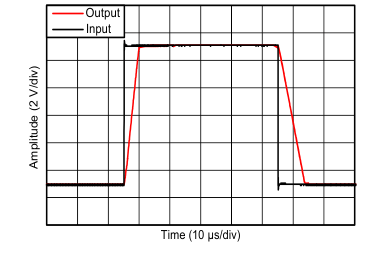
Figure 7-47 Large Signal Step Response
GUID-4435C150-5C4C-4C32-94AD-133A1D481CC0-low.gif
 
Figure 7-49 Differential-Mode EMI Rejection Ratio
GUID-2000F91B-A152-48EB-B001-6314FA99FA6D-low.gif
VS = 5 V G = 1
Figure 7-51 Input Common-Mode Voltage vs Output Voltage
GUID-93ED5770-B433-40FD-9305-76B7524F258A-low.gif
VS = ±5 V VREF = 0 V
Figure 7-53 Input Common-Mode Voltage vs Output Voltage
GUID-2B256081-0DF1-45C1-BAC1-642F184DA9F3-low.gif
N = 45 Mean = 0.0357 µV/°C Std. Dev. = 0.099 µV/°C
Figure 7-2 Typical Distribution of Input Stage Offset Voltage Drift
GUID-4B711EDD-9208-417B-9DB5-BA0C90121E81-low.gif
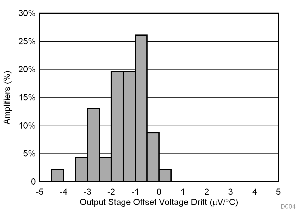
N = 45 Mean = –1.49 µV/°C Std. Dev. = 0.89 µV/°C
Figure 7-4 Typical Distribution of Output Stage Offset Voltage Drift
GUID-378C443E-5EC5-49C7-94A1-2E6810E20511-low.gif
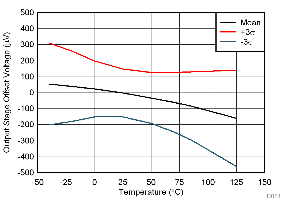
45 units, 1 wafer lots
Figure 7-6 Output Stage Offset Voltage vs Temperature
GUID-FFDB2CD6-6C92-4607-AE83-CFFB6148DF49-low.gif
N = 94 Mean = –27.65 pA Std. Dev. = 52.58 pA
TA = 90°C
Figure 7-8 Typical Distribution of Input Bias Current
N = 94 G = 1
Figure 7-10 Input Bias Current vs Temperature
GUID-7CC48332-4F54-4AB3-8408-A668C4AD91EE-low.gif
N = 94 Mean = 3.23 µV/V Std. Dev. = 5.38 µV/V
G = 1
Figure 7-12 Typical CMRR Distribution
GUID-20356CB4-1F2F-4C16-8F64-88F606873F90-low.gif
5 typical units G = 1
 
Figure 7-14 CMRR vs Temperature
GUID-C9D4B783-98A5-449D-B365-50A67172862C-low.gif
VS = 36 V
Figure 7-16 Input Current vs Input Overvoltage
GUID-496F96CA-24CF-43C9-9972-AD973848B8F4-low.gif
1-kΩ source imbalance
Figure 7-18 CMRR vs Frequency (RTI)
GUID-23CEE3ED-5D66-4871-BCF1-EA20C1BE48E9-low.gif
 
Figure 7-20 Negative PSRR vs Frequency (RTI)
GUID-5F2322A8-5CC7-414A-BCE2-B0A092AF2AF2-low.gifFigure 7-22 Voltage Noise Spectral Density vs Frequency (RTI)
GUID-A6A04615-3EB4-48A1-93A4-ACCAE0488484-low.gif
G = 1
Figure 7-24 0.1-Hz to 10-Hz RTI Voltage Noise
GUID-EB7E31CE-3FBB-4DDA-9C31-996F0F1726C5-low.gif
 
Figure 7-26 0.1-Hz to 10-Hz RTI Current Noise
GUID-E58C950C-41E1-4814-B3A7-484DEDC1B965-low.gif
N = 94 Mean = –48 ppm Std. Dev. = 58 ppm
G = 1
Figure 7-28 Typical Distribution of Gain Error,
G = 1
GUID-DB384ECC-EDDD-45B1-82D6-587F40622937-low.gif
G = 1
 
Figure 7-30 Gain Error vs Temperature
GUID-3F5023A7-CCB4-4E34-9B9D-F35F15568C5B-low.gif
 
Figure 7-32 Supply Current vs Temperature
GUID-99D06F92-B7CC-4B0F-B1A7-98FB6F394B0D-low.gif
G = 10
Figure 7-34 Gain Nonlinearity
GUID-2CA48303-45AD-45CC-A7AF-78CC0E751CE9-low.gif
 
Figure 7-36 Offset Voltage vs Positive Common-Mode Voltage
GUID-9379DB7E-1BFC-4806-A873-711941E447D9-low.gif
 
Figure 7-38 Negative Output Voltage Swing vs Output Current
GUID-CC2D8623-45EF-4F49-8E14-4F7553FFF0F0-low.gif
 
Figure 7-40 Large-Signal Frequency Response
GUID-D2E66254-8386-43D8-976E-472144F1974E-low.gif
 
 
Figure 7-42 Overshoot vs Capacitive Loads
GUID-EF9DB0F7-5534-415B-BD36-D1CEEE1179BC-low.gif
G = 10 RL = 10 kΩ CL = 100 pF
Figure 7-44 Small-Signal Response
GUID-1D4B02C3-388F-4467-851E-868DC6A64545-low.gif
G = 1000 RL = 10 kΩ CL = 100 pF
Figure 7-46 Small-Signal Response
GUID-677D8D37-72E3-4AF2-84C3-3E81894C6C37-low.gif
 
 
Figure 7-48 Closed-Loop Output Impedance
GUID-53387BFB-DF88-4D93-B27F-2FF70F1D1C11-low.gif
 
Figure 7-50 Common-Mode EMI Rejection Ratio
GUID-DDA96265-A963-4B0A-B930-3D60C8C5FB72-low.gif
VS = 5 V G = 100
Figure 7-52 Input Common-Mode Voltage vs Output Voltage
GUID-5EE687FF-30B9-4327-B4F6-50B3EAF60125-low.gif
VS = ±15 V VREF = 0 V
Figure 7-54 Input Common-Mode Voltage vs Output Voltage