SBOSA75B July 2021 – November 2021 INA823
PRODUCTION DATA
- 1 Features
- 2 Applications
- 3 Description
- 4 Revision History
- 5 Device Comparison Table
- 6 Pin Configuration and Functions
- 7 Specifications
- 8 Detailed Description
- 9 Application and Implementation
- 10Power Supply Recommendations
- 11Layout
- 12Device and Documentation Support
- 13Mechanical, Packaging, and Orderable Information
Package Options
Mechanical Data (Package|Pins)
Thermal pad, mechanical data (Package|Pins)
Orderable Information
3 Description
The INA823 is an integrated instrumentation amplifier that offers low power consumption and operates over a wide, single-supply or dual-supply range. A single external resistor sets any gain from 1 to 10,000. The device provides low input offset voltage, low offset voltage drift, low input bias current, and low current noise while remaining cost-effective. Additional circuitry protects the inputs against overvoltage up to ±60 V.
The INA823 is optimized to provide a high common-mode rejection ratio. At G = 1, the common-mode rejection ratio exceeds 84 dB across the full input common-mode range. The INA823 has a wide common-mode voltage range as low as 150-mV below negative supply. The device is designed for low-voltage operation from a 2.7-V single supply, and dual supplies up to ±18 V. The low power and single supply operation enable hand-held, battery-operated systems.
| PART NUMBER | PACKAGE(1) | BODY SIZE (NOM) |
|---|---|---|
| INA823 | SOIC (8) | 4.90 mm × 3.91 mm |
| VSSOP (8) | 3.00 mm x 3.00 mm |
 INA823 Simplified Internal Schematic
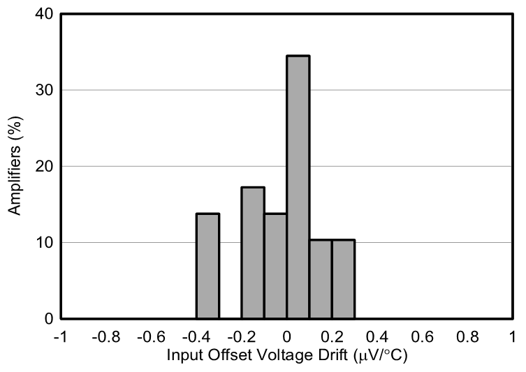
 Typical Distribution of
 Input Stage Offset Voltage Drift