SBOS562G August   2011  – June 2020 INA826

PRODUCTION DATA.  

  1. Features
  2. Applications
  3. Description
    1.     Device Images
      1.      General-Purpose Instrumentation Amplifier
  4. Revision History
  5. Device Comparison Table
  6. Pin Configuration and Functions
    1.     Pin Functions
  7. Specifications
    1. 7.1 Absolute Maximum Ratings
    2. 7.2 ESD Ratings
    3. 7.3 Recommended Operating Conditions
    4. 7.4 Thermal Information
    5. 7.5 Electrical Characteristics
    6. 7.6 Typical Characteristics
  8. Detailed Description
    1. 8.1 Overview
    2. 8.2 Functional Block Diagram
    3. 8.3 Feature Description
      1. 8.3.1  Inside the INA826
      2. 8.3.2  Setting the Gain
        1. 8.3.2.1 Gain Drift
      3. 8.3.3  Offset Trimming
      4. 8.3.4  Input Common-Mode Range
      5. 8.3.5  Input Protection
      6. 8.3.6  Input Bias Current Return Path
      7. 8.3.7  Reference Terminal
      8. 8.3.8  Dynamic Performance
      9. 8.3.9  Operating Voltage
        1. 8.3.9.1 Low-Voltage Operation
      10. 8.3.10 Error Sources
    4. 8.4 Device Functional Modes
  9. Application and Implementation
    1. 9.1 Application Information
    2. 9.2 Typical Application
      1. 9.2.1 Design Requirements
      2. 9.2.2 Detailed Design Procedure
      3. 9.2.3 Application Curves
    3. 9.3 System Examples
      1. 9.3.1 Circuit Breaker
      2. 9.3.2 Programmable Logic Controller (PLC) Input
      3. 9.3.3 Using TINA-TI SPICE-Based Analog Simulation Program With the INA826
  10. 10Power Supply Recommendations
  11. 11Layout
    1. 11.1 Layout Guidelines
      1. 11.1.1 CMRR vs Frequency
    2. 11.2 Layout Example
  12. 12Device and Documentation Support
    1. 12.1 Documentation Support
      1. 12.1.1 Related Documentation
    2. 12.2 Receiving Notification of Documentation Updates
    3. 12.3 Support Resources
    4. 12.4 Trademarks
    5. 12.5 Electrostatic Discharge Caution
    6. 12.6 Glossary
  13. 13Mechanical, Packaging, and Orderable Information

Package Options

Mechanical Data (Package|Pins)
Thermal pad, mechanical data (Package|Pins)
Orderable Information

Typical Application

Figure 63 shows a three-terminal programmable-logic controller (PLC) design for the INA826. This PLC reference design accepts inputs of ±10 V or ±20 mA. The output is a single-ended voltage of 2.5 V ±2.3 V (or 200 mV to 4.8 V). Many PLCs typically have these input and output ranges.
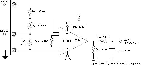
INA826 ai_3-term_plc_bos562.gifFigure 63. Three-Terminal PLC Design