SBOS946 September 2020 INA848
PRODUCTION DATA
- 1 Features
- 2 Applications
- 3 Description
- 4 Revision History
- 5 Device Comparison Table
- 6 Pin Configuration and Functions
- 7 Specifications
- 8 Detailed Description
- 9 Application and Implementation
- 10Power Supply Recommendations
- 11Layout
- 12Device and Documentation Support
- 13Mechanical, Packaging, and Orderable Information
Package Options
Mechanical Data (Package|Pins)
- D|8
Thermal pad, mechanical data (Package|Pins)
Orderable Information
3 Description
The INA848 is a fixed-gain instrumentation amplifier optimized for high-precision measurements, such as very-small, fast, differential input signals. TI's super-beta topology provides a very low input bias current and current noise. The well-matched transistors help achieve a very low offset and offset drift. Matching of the internal resistors yields a high common-mode rejection ratio of 132 dB across the full input-voltage range, and a very low gain drift error of 5 ppm/⁰C (max).
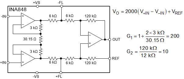
The current-feedback topology of the INA848 produces a wide bandwidth of 2.8 MHz at a fixed gain of 2000, thereby eliminating the need for subsequent gain stages. The very-low noise floor of 1.3 nV/√Hz minimizes the impact on the equivalent number of bits (ENOB) when interfacing with high-resolution analog-to-digital converters (ADCs). The INA848 provides the flexibility of adding filters between the gain stages (pins 2 and 3) to maintain an adequate signal integrity.
These unique features of the INA848 make this device an excellent choice for applications requiring high-precision measurements, such as high-end medical instrumentation, electroencephalography, vibration sensing, and displacement measurements.
This device is designed for 8-V to 36-V single supplies, or ±4-V to ±18-V on dual supplies.
| PART NUMBER(1) | PACKAGE | BODY SIZE (NOM) |
|---|---|---|
| INA848 | SOIC (8) | 4.90 mm × 3.91 mm |
 INA848 Simplified Internal Schematic
 Typical Distribution of Input Offset
Voltage