SBOS945B November 2020 – April 2021 INA849
PRODUCTION DATA
- 1 Features
- 2 Applications
- 3 Description
- 4 Revision History
- 5 Device Comparison Table
- 6 Pin Configuration and Functions
- 7 Specifications
- 8 Detailed Description
- 9 Application and Implementation
- 10Power Supply Recommendations
- 11Layout
- 12Device and Documentation Support
- 13Mechanical, Packaging, and Orderable Information
Package Options
Mechanical Data (Package|Pins)
Thermal pad, mechanical data (Package|Pins)
Orderable Information
9.1.1 Reference Pin
The output voltage of the INA849 is developed with respect to the voltage on reference pin REF.
Use the REF pin to offset the output signal to a precise midsupply level. Typically, this offset is 2.5 V in a 5-V supply environment. To accomplish this level shift, a voltage source must be connected to the REF pin to level-shift the output so that the INA849 drives a single-supply analog-to-digital converter (ADC).
For dual-supply operation, the reference pin is typically connected to the low-impedance system ground.
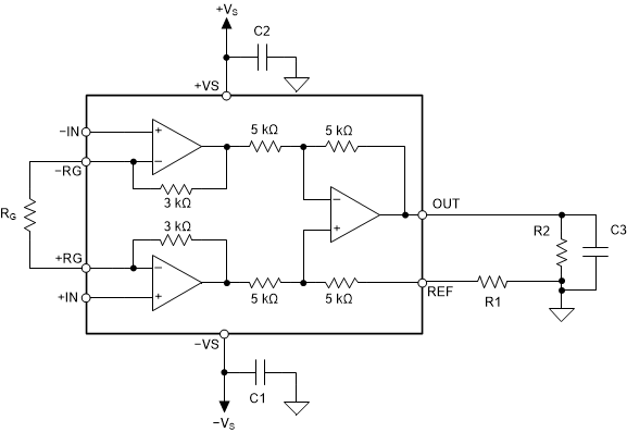
The voltage source applied to the reference pin must have a low output impedance. As shown in Figure 9-1, any resistance at the reference pin (shown as RREF) is in series with an internal 5-kΩ resistor that creates an imbalance in the four resistors of the internal difference amplifier.
 Figure 9-1 Parasitic Resistance Shown at
the Reference Pin
Figure 9-1 Parasitic Resistance Shown at
the Reference PinThis imbalance results in a degraded common-mode rejection ratio (CMRR). Figure 9-2 shows how the common-mode rejection ratio degrades depending on the source resistance on the reference pin. For best performance, keep the dc CMRR greater than 100 dB by keeping the source impedance to the REF pin (represented as R1) to less than 0.1 Ω.
 Figure 9-2 Effect of Parasitic Resistance
at the Reference Pin
Figure 9-2 Effect of Parasitic Resistance
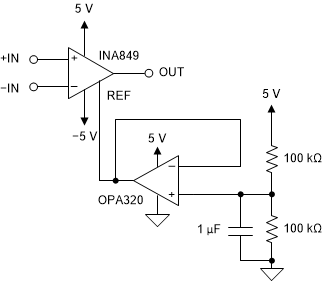
at the Reference PinVoltage-reference devices are an excellent option for providing a low-impedance voltage source for the reference pin. However, if a resistor voltage divider generates a reference voltage, the divider must be buffered by an op amp (as Figure 9-3 shows) to avoid CMRR degradation.
 Figure 9-3 Using an
Op Amp to Buffer Reference Voltages