SBOS999A March 2022 – October 2022 INA851
PRODUCTION DATA
- 1 Features
- 2 Applications
- 3 Description
- 4 Revision History
- 5 Related Products
- 6 Pin Configuration and Functions
- 7 Specifications
- 8 Detailed Description
-
9 Application and Implementation
- 9.1 Application Information
- 9.2 Typical Applications
- 9.3 Power Supply Recommendations
- 9.4 Layout
- 10Device and Documentation Support
- 11Mechanical, Packaging, and Orderable Information
Package Options
Mechanical Data (Package|Pins)
- RGT|16
Thermal pad, mechanical data (Package|Pins)
- RGT|16
Orderable Information
9.2.2.2 Application Curves
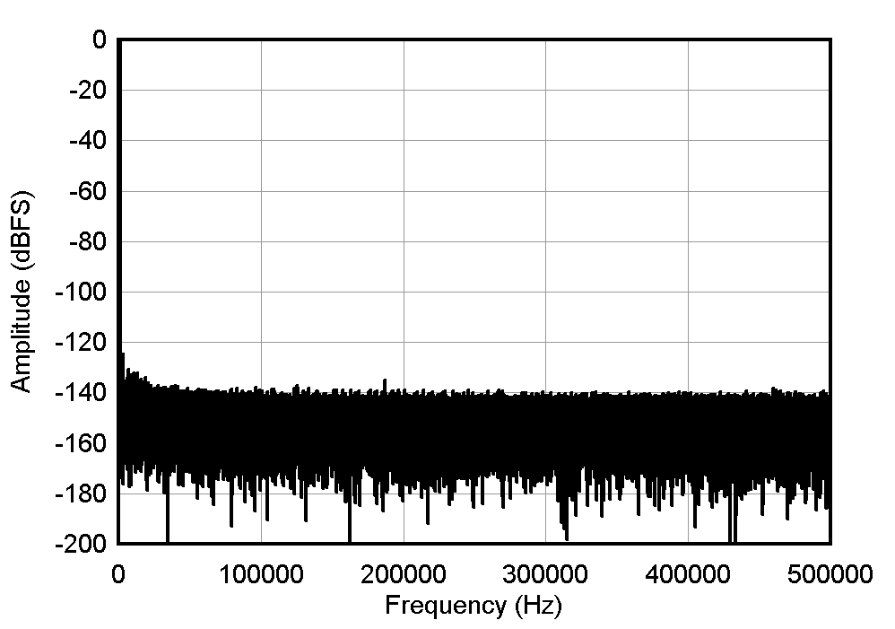
Table 9-2 show the typical signal-to-noise (SNR) and total harmonic distortion (THD) of the INA851 driving the ADS8900B SAR ADC at full-scale range and at different gain configurations. The RC filter combination (RFIL, CFIL) shown in Figure 9-6 helps attenuate the nonlinear charge kickback of the ADC and optimize for best THD performance. The combination of the RC filter and the feedback capacitor CFB allow for the best trade-off between harmonic distortion and maintaining stability of the FDA. Low voltage-coefficient C0G capacitors are used everywhere in the signal path (CFB, CFIL) for the low-distortion properties.
For other bandwidth requirements, adjust the feedback capacitor accordingly, and verify the circuit performance using a SPICE simulation using the INA851 TINA-TI™ SPICE Model. The amplifier output voltage must settle within the ADC bit accuracy during the ADC acquisition time window. Verify the desired circuit is stable; that is, the FDA has more than a 45º phase margin.
| INPUT AMPLITUDE (Vpk) | RG RESISTOR (Ω) | GIN (V/V) | GOUT (V/V) | SNR (dB) | THD (dB) | ENOB (Bits) |
|---|---|---|---|---|---|---|
| 23.7378 | None | 1 | 0.2 | 100.7 | –117.3 | 16.42 |
| 4.7476 | None | 1 | 1 | 100.6 | –122.7 | 16.41 |
| 0.2374 | 316 | 20 | 1 | 99.1 | –112.0 | 16.10 |
| 0.0475 | 60.4 | 100 | 1 | 91.1 | –99.0 | 14.64 |

| G = 0.2 V/V, fIN = 1 kHz, SNR = 100.73 dB, THD = –117.28 dB |

| G = 1 V/V, fIN = 1 kHz, SNR = 100.6 dB, THD = –122.74 dB |