SBOS938C October 2018 – June 2020 INA901-SP
PRODUCTION DATA.
- 1 Features
- 2 Applications
- 3 Description
- 4 Revision History
- 5 Pin Configuration and Functions
- 6 Specifications
- 7 Detailed Description
- 8 Application and Implementation
- 9 Power Supply Recommendations
- 10Layout
- 11Device and Documentation Support
- 12Mechanical, Packaging, and Orderable Information
Package Options
Mechanical Data (Package|Pins)
- HKX|8
Thermal pad, mechanical data (Package|Pins)
Orderable Information
7.4.2.3 Low VSENSE Case 1: VSENSE < 20 mV, –15 V ≤ VCM < 0; and Low VSENSE Case 3: VSENSE < 20 mV,
VS < VCM ≤ 65 V
Although the INA901-SP is not designed for accurate operation in either of these regions, some applications are exposed to these conditions. For example, when monitoring power supplies that are switched on and off while VS is still applied to the INA901-SP, knowing what the behavior of the device is in these regions is important.
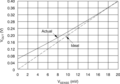
When VSENSE approaches 0 mV, in these VCM regions, the device output accuracy degrades. A larger-than-normal offset can appear at the current shunt monitor output with a typical maximum value of VOUT = 60 mV for VSENSE = 0 mV. When VSENSE approaches 20 mV, VOUT returns to the expected output value with accuracy as specified in the Electrical Characteristics table. Figure 17 shows this effect using the INA901-SP (gain = 20).
