SBOS074E September 1997 – June 2018 ISO124
PRODUCTION DATA.
- 1 Features
- 2 Applications
- 3 Description
- 4 Revision History
- 5 Pin Configuration and Functions
- 6 Specifications
- 7 Detailed Description
-
8 Application and Implementation
- 8.1 Application Information
- 8.2
Typical Applications
- 8.2.1 Output Filters
- 8.2.2 Battery Monitor
- 8.2.3 Programmable Gain Amplifier
- 8.2.4 Thermocouple Amplifier
- 8.2.5 Isolated 4-mA to 20-mA Instrument Loop
- 8.2.6 Single-Supply Operation of the ISO124 Isolation Amplifier
- 8.2.7 Input-Side Powered ISO Amplifier
- 8.2.8 Powered ISO Amplifier With Three-Port Isolation
- 9 Power Supply Recommendations
- 10Layout
- 11Device and Documentation Support
- 12Mechanical, Packaging, and Orderable Information
Package Options
Refer to the PDF data sheet for device specific package drawings
Mechanical Data (Package|Pins)
- NVF|8
- DVA|8
Thermal pad, mechanical data (Package|Pins)
Orderable Information
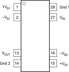
5 Pin Configuration and Functions
NVF Package
16-Pin PDIP
Top View

DVA Package
28-Pin SOIC
Top View

Pin Functions
| PIN | I/O | DESCRIPTION | ||
|---|---|---|---|---|
| NAME | PDIP | SOIC | ||
| Gnd 1 | 16 | 28 | — | High-side ground reference |
| Gnd 2 | 8 | 14 | — | Low-side ground reference |
| VIN | 15 | 27 | I | High-side analog input |
| VOUT | 7 | 13 | O | Low-side analog output |
| +VS1 | 1 | 1 | — | High-side positive analog supply |
| –VS1 | 2 | 2 | — | High-side negative analog supply |
| +VS2 | 9 | 15 | — | Low-side positive analog supply |
| –VS2 | 10 | 16 | — | Low-side negative analog supply |