SLLSF22H April 2018 – June 2024 ISO1410 , ISO1412 , ISO1430 , ISO1432 , ISO1450 , ISO1452
PRODUCTION DATA
- 1
- 1 Features
- 2 Applications
- 3 Description
- 4 Description Continued
- 5 Device Comparison Table
- 6 Pin Configuration and Functions
-
7 Specifications
- 7.1 Absolute Maximum Ratings
- 7.2 ESD Ratings
- 7.3 Recommended Operating Conditions
- 7.4 Thermal Information
- 7.5 Power Ratings
- 7.6 Insulation Specifications
- 7.7 Safety-Related Certifications
- 7.8 Safety Limiting Values
- 7.9 Electrical Characteristics: Driver
- 7.10 Electrical Characteristics: Receiver
- 7.11 Supply Current Characteristics: Side 1 (ICC1)
- 7.12 Supply Current Characteristics: Side 2 (ICC2)
- 7.13 Switching Characteristics: Driver
- 7.14 Switching Characteristics: Receiver
- 7.15 Insulation Characteristics Curves
- 7.16 Typical Characteristics
- 8 Parameter Measurement Information
- 9 Detailed Description
- 10Application and Implementation
- 11Power Supply Recommendations
- 12Layout
- 13Device and Documentation Support
- 14Revision History
- 15Mechanical, Packaging, and Orderable Information
Package Options
Refer to the PDF data sheet for device specific package drawings
Mechanical Data (Package|Pins)
- DW|16
Thermal pad, mechanical data (Package|Pins)
- DW|16
Orderable Information
Pin Functions: Half-Duplex Device
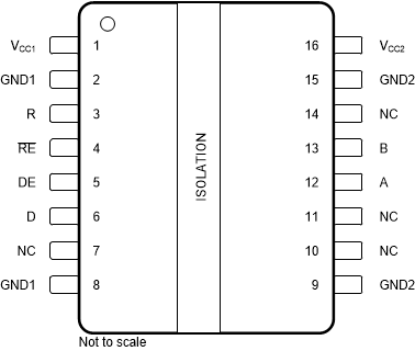
 Figure 6-2 DW Package16-Pin SOICHalf-Duplex Device Top View
| PIN | Type(1) | DESCRIPTION | |
|---|---|---|---|
| NAME | NO. | ||
| A | 12 | I/O | Transceiver non-inverting input or output (I/O) on the bus side |
| B | 13 | I/O | Transceiver inverting input or output (I/O) on the bus side |
| D | 6 | I | Driver input |
| DE | 5 | I | Driver enable. This pin enables the driver output when high and disables the driver output when low or open. |
| GND1(2) | 2 | — | Ground connection for VCC1 |
| GND1(2) | 8 | — | Ground connection for VCC1 |
| GND2(2) | 9 | — | Ground connection for VCC2 |
| GND2(2) | 15 | — | Ground connection for VCC2 |
| NC(3) | 7 | — | No internal connection |
| NC(3) | 10 | — | No internal connection |
| NC(3) | 11 | — | No internal connection |
| NC(3) | 14 | — | No internal connection |
| R | 3 | O | Receiver output |
| RE | 4 | I | Receiver enable. This pin disables the receiver output when high or open and enables the receiver output when low. |
| VCC1 | 1 | — | Logic-side power supply |
| VCC2 | 16 | — | Transceiver-side power supply |
(1) I = Input, O = Output, I/O = Input or Output
(2) For Logic side, both Pin 2 and Pin 8 must be connected to GND1.
For Bus side, both Pin 9 and Pin 15 must be connected to GND2.
(3) Device functionality is not affected if NC pins are connected
to supply or ground on PCB