SLLSF22H April 2018 – June 2024 ISO1410 , ISO1412 , ISO1430 , ISO1432 , ISO1450 , ISO1452
PRODUCTION DATA
- 1
- 1 Features
- 2 Applications
- 3 Description
- 4 Description Continued
- 5 Device Comparison Table
- 6 Pin Configuration and Functions
-
7 Specifications
- 7.1 Absolute Maximum Ratings
- 7.2 ESD Ratings
- 7.3 Recommended Operating Conditions
- 7.4 Thermal Information
- 7.5 Power Ratings
- 7.6 Insulation Specifications
- 7.7 Safety-Related Certifications
- 7.8 Safety Limiting Values
- 7.9 Electrical Characteristics: Driver
- 7.10 Electrical Characteristics: Receiver
- 7.11 Supply Current Characteristics: Side 1 (ICC1)
- 7.12 Supply Current Characteristics: Side 2 (ICC2)
- 7.13 Switching Characteristics: Driver
- 7.14 Switching Characteristics: Receiver
- 7.15 Insulation Characteristics Curves
- 7.16 Typical Characteristics
- 8 Parameter Measurement Information
- 9 Detailed Description
- 10Application and Implementation
- 11Power Supply Recommendations
- 12Layout
- 13Device and Documentation Support
- 14Revision History
- 15Mechanical, Packaging, and Orderable Information
Package Options
Refer to the PDF data sheet for device specific package drawings
Mechanical Data (Package|Pins)
- DW|16
Thermal pad, mechanical data (Package|Pins)
- DW|16
Orderable Information
8 Parameter Measurement Information
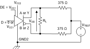 Figure 8-1 Driver Voltages
A. RL = 100 Ω for
RS422, RL = 54 Ω for RS-485
Figure 8-2 Driver Voltages
A. CL includes
fixture and instrumentation capacitance.
Figure 8-3 Driver Switching
Specifications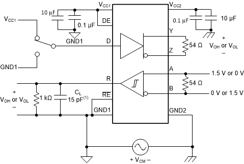
A. Includes probe and fixture
capacitance.
Figure 8-4 Common Mode Transient
Immunity (CMTI)—Full Duplex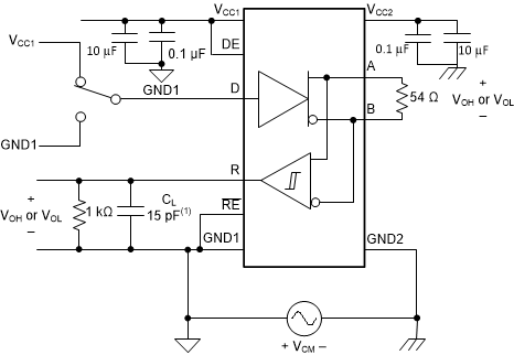
A. Includes probe and
fixture capacitance.
Figure 8-5 Common Mode Transient Immunity (CMTI)—Half Duplex
A. CL includes
fixture and instrumentation capacitance
Figure 8-6 Driver Enable and Disable
Times 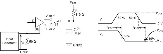 Figure 8-7 Driver Enable and Disable
Times
A. CL includes
fixture and instrumentation capacitance.
Figure 8-8 Receiver Switching
Specifications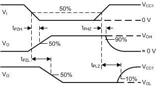 Figure 8-9 Receiver Enable and
Disable Times
  Figure 8-10 Receiver Enable and
Disable Times
A. The driver should not sustain
any damage with this configuration.
Figure 8-11 Short-Circuit Current
Limiting