SLLSF22H April 2018 – June 2024 ISO1410 , ISO1412 , ISO1430 , ISO1432 , ISO1450 , ISO1452
PRODUCTION DATA
- 1
- 1 Features
- 2 Applications
- 3 Description
- 4 Description Continued
- 5 Device Comparison Table
- 6 Pin Configuration and Functions
-
7 Specifications
- 7.1 Absolute Maximum Ratings
- 7.2 ESD Ratings
- 7.3 Recommended Operating Conditions
- 7.4 Thermal Information
- 7.5 Power Ratings
- 7.6 Insulation Specifications
- 7.7 Safety-Related Certifications
- 7.8 Safety Limiting Values
- 7.9 Electrical Characteristics: Driver
- 7.10 Electrical Characteristics: Receiver
- 7.11 Supply Current Characteristics: Side 1 (ICC1)
- 7.12 Supply Current Characteristics: Side 2 (ICC2)
- 7.13 Switching Characteristics: Driver
- 7.14 Switching Characteristics: Receiver
- 7.15 Insulation Characteristics Curves
- 7.16 Typical Characteristics
- 8 Parameter Measurement Information
- 9 Detailed Description
- 10Application and Implementation
- 11Power Supply Recommendations
- 12Layout
- 13Device and Documentation Support
- 14Revision History
- 15Mechanical, Packaging, and Orderable Information
Package Options
Refer to the PDF data sheet for device specific package drawings
Mechanical Data (Package|Pins)
- DW|16
Thermal pad, mechanical data (Package|Pins)
- DW|16
Orderable Information
10.1 Application Information
The ISO14xx devices are designed for bidirectional data transfer on multipoint RS-485 networks. The design of each RS-485 node in the network requires an ISO14xx device and an isolated power supply as shown in Figure 10-3.
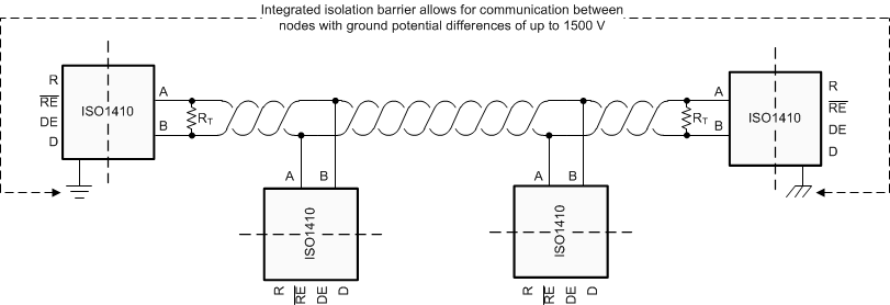
An RS-485 bus has multiple transceivers that connect in parallel to a bus cable. Both cable ends are terminated with a termination resistor, RT, to remove line reflections. The value of RT matches the characteristic impedance, Z0, of the cable. This method, known as parallel termination, lets higher data rates be used over a longer cable length.
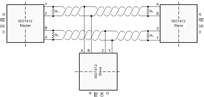
Full-duplex implementation, as shown in Figure 10-1, requires two signal pairs (four wires). Full-duplex implementation lets each node to transmit data on one pair while simultaneously receiving data on the other pair. In half-duplex implementation, as shown in Figure 10-2, the driver and receiver enable pins let any node at any given moment be configured in either transmit or receive mode which decreases cable requirements.
 Figure 10-1 Typical RS-485 Network With Full-Duplex Isolated Transceivers
 Figure 10-2 Typical RS-485 Network With Half-Duplex Isolated Transceivers