SLLSF22H April 2018 – June 2024 ISO1410 , ISO1412 , ISO1430 , ISO1432 , ISO1450 , ISO1452
PRODUCTION DATA
- 1
- 1 Features
- 2 Applications
- 3 Description
- 4 Description Continued
- 5 Device Comparison Table
- 6 Pin Configuration and Functions
-
7 Specifications
- 7.1 Absolute Maximum Ratings
- 7.2 ESD Ratings
- 7.3 Recommended Operating Conditions
- 7.4 Thermal Information
- 7.5 Power Ratings
- 7.6 Insulation Specifications
- 7.7 Safety-Related Certifications
- 7.8 Safety Limiting Values
- 7.9 Electrical Characteristics: Driver
- 7.10 Electrical Characteristics: Receiver
- 7.11 Supply Current Characteristics: Side 1 (ICC1)
- 7.12 Supply Current Characteristics: Side 2 (ICC2)
- 7.13 Switching Characteristics: Driver
- 7.14 Switching Characteristics: Receiver
- 7.15 Insulation Characteristics Curves
- 7.16 Typical Characteristics
- 8 Parameter Measurement Information
- 9 Detailed Description
- 10Application and Implementation
- 11Power Supply Recommendations
- 12Layout
- 13Device and Documentation Support
- 14Revision History
- 15Mechanical, Packaging, and Orderable Information
Package Options
Refer to the PDF data sheet for device specific package drawings
Mechanical Data (Package|Pins)
- DW|16
Thermal pad, mechanical data (Package|Pins)
- DW|16
Orderable Information
3 Description
The ISO14xx devices are galvanically-isolated differential line transceivers for TIA/EIA RS-485 and RS-422 applications. These noise-immune transceivers are designed to operate in harsh industrial environments. The bus pins of these devices can endure high levels of IEC electrostatic discharge (ESD) and IEC electrical fast transient (EFT) events which eliminates the need for additional components on bus for system-level protection. The devices are available for both basic and reinforced isolation (see Reinforced and Basic Isolation Options).
| PART NUMBER | PACKAGE(1) | PACKAGE SIZE(2) |
|---|---|---|
| ISO1410, ISO1410B | SOIC (16) | 10.30mm × 10.30mm |
| ISO1412, ISO1412B | ||
| ISO1430, ISO1430B | ||
| ISO1432, ISO1432B | ||
| ISO1450, ISO1450B | ||
| ISO1452, ISO1452B |
| Feature | ISO14xx | ISO14xxB |
|---|---|---|
| Protection level | Reinforced | Basic |
| Surge test voltage per VDE | 10000VPK | 6000VPK |
| Isolation rating per UL | 5000VRMS | 5000VRMS |
| Working voltage per VDE | 1060VRMS / 1500VPK |
1060VRMS / 1500VPK |
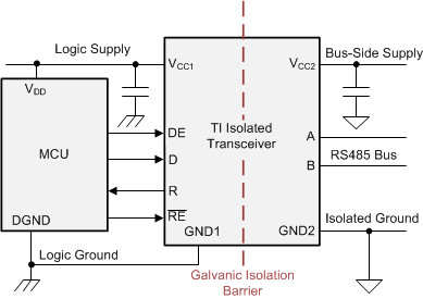
 Simplified Application Schematic