SLLSEN5C june 2015 – may 2023 ISO5851
PRODUCTION DATA
- 1
- 1 Features
- 2 Applications
- 3 Description
- 4 Revision History
- 5 Description (continued)
- 6 Pin Configuration and Function
-
7 Specifications
- 7.1 Absolute Maximum Ratings
- 7.2 ESD Ratings
- 7.3 Recommended Operating Conditions
- 7.4 Thermal Information
- 7.5 Power Ratings
- 7.6 Insulation Characteristics
- 7.7 Safety-Related Certifications
- 7.8 Safety Limiting Values
- 7.9 Electrical Characteristics
- 7.10 Switching Characteristics
- 7.11 Insulation Characteristics Curves
- 7.12 Typical Characteristics
- 8 Parameter Measurement Information
- 9 Detailed Description
-
10Application and Implementation
- 10.1 Application Information
- 10.2
Typical Applications
- 10.2.1 Design Requirements
- 10.2.2
Detailed Design Procedure
- 10.2.2.1 Recommended ISO5851 Application Circuit
- 10.2.2.2 FLT and RDY Pin Circuitry
- 10.2.2.3 Driving the Control Inputs
- 10.2.2.4 Local Shutdown and Reset
- 10.2.2.5 Global-Shutdown and Reset
- 10.2.2.6 Auto-Reset
- 10.2.2.7 DESAT Pin Protection
- 10.2.2.8 DESAT Diode and DESAT Threshold
- 10.2.2.9 Determining the Maximum Available, Dynamic Output Power, POD-max
- 10.2.2.10 Example
- 10.2.2.11 Higher Output Current Using an External Current Buffer
- 10.2.3 Application Curves
- 11Power Supply Recommendations
- 12Layout
- 13Device and Documentation Support
- 14Mechanical, Packaging, and Orderable Information
Package Options
Mechanical Data (Package|Pins)
- DW|16
Thermal pad, mechanical data (Package|Pins)
- DW|16
Orderable Information
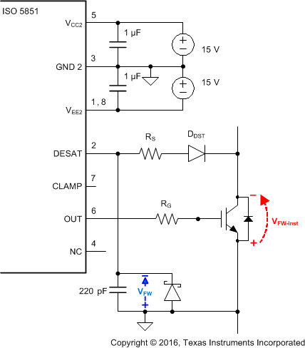
10.2.2.7 DESAT Pin Protection
Switching inductive loads causes large instantaneous forward voltage transients across the freewheeling diodes of IGBTs. These transients result in large negative voltage spikes on the DESAT pin which draw substantial current out of the device. To limit this current below damaging levels, a 100-Ω to 1-kΩ resistor is connected in series with the DESAT diode.
Further protection is possible through an optional Schottky diode, whose low forward voltage assures clamping of the DESAT input to GND2 potential at low voltage levels.
 Figure 10-8 DESAT Pin Protection With Series Resistor and Schottky Diode