6 Specifications
6.1 Absolute Maximum Ratings(1)
|
MIN |
MAX |
UNIT |
| VCC1, VCC2 |
Supply voltage(2) |
–0.5 |
6 |
V |
| INx, ENx, OUTx |
Voltage |
–0.5 |
VCC+ 0.5(3) |
V |
| IO |
Output current |
–15 |
15 |
mA |
| TJ |
Maximum junction temperature |
|
150 |
°C |
| Tstg |
Storage temperature |
–65 |
150 |
°C |
(1) Stresses beyond those listed under Absolute Maximum Ratings may cause permanent damage to the device. These are stress ratings only, and functional operation of the device at these or any other conditions beyond those indicated under
Recommended Operating Conditions is not implied. Exposure to absolute-maximum-rated conditions for extended periods may affect device reliability.
(2) All voltage values except differential I/O bus voltages are with respect to the local ground terminal (GND1 or GND2) and are peak voltage values.
(3) Maximum voltage must not exceed 6 V
6.2 ESD Ratings
|
VALUE |
UNIT |
| V(ESD) |
Electrostatic discharge |
Human body model (HBM), per ANSI/ESDA/JEDEC JS-001(1) |
±4000 |
V |
| Charged-device model (CDM), per JEDEC specification JESD22-C101(2) |
±1500 |
(1) JEDEC document JEP155 states that 500-V HBM allows safe manufacturing with a standard ESD control process.
(2) JEDEC document JEP157 states that 250-V CDM allows safe manufacturing with a standard ESD control process.
6.3 Recommended Operating Conditions
|
|
MIN |
NOM |
MAX |
UNIT |
| VCC1, VCC2 |
Supply voltage |
2.7 |
|
5.5 |
V |
| IOH |
High-level output current (VCC ≥ 3.0 V) |
–4 |
|
|
mA |
| High-level output current (VCC < 3.0 V) |
–2 |
|
|
| IOL |
Low-level output current |
|
|
4 |
mA |
| VIH |
High-level input voltage |
2 |
|
5.5 |
V |
| VIL |
Low-level input voltage |
0 |
|
0.8 |
| tui |
Input pulse duration (VCC ≥ 4.5V) |
20 |
|
|
ns |
| tui |
Input pulse duration (VCC < 4.5V) |
25 |
|
|
| 1 / tui |
Signaling rate (VCC ≥ 4.5V) |
0 |
|
50 |
Mbps |
| 1 / tui |
Signaling rate (VCC < 4.5V) |
0 |
|
40 |
| TA |
Ambient temperature |
–40 |
25 |
125 |
°C |
| TJ |
Junction temperature |
–40 |
|
136 |
6.4 Thermal Information
| THERMAL METRIC(1) |
ISO7131, ISO714x |
UNIT |
| DBQ |
| 16 PINS |
| RθJA |
Junction-to-ambient thermal resistance |
104.5 |
°C/W |
| RθJC(top) |
Junction-to-case(top) thermal resistance |
57.8 |
°C/W |
| RθJB |
Junction-to-board thermal resistance |
46.8 |
°C/W |
| ψJT |
Junction-to-top characterization parameter |
18.3 |
°C/W |
| ψJB |
Junction-to-board characterization parameter |
46.4 |
°C/W |
(1) For more information about traditional and new thermal metrics, see the
IC Package Thermal Metrics application report,
SPRA953.
6.5 Power Dissipation Ratings
|
TEST CONDITIONS |
VALUE |
UNIT |
| PD |
Device power dissipation |
VCC1 = VCC2 = 5.5 V, TJ = 150°C, CL = 15 pF
Input a 25-MHz, 50% duty cycle square wave |
150 |
mW |
6.6 Electrical Characteristics: VCC1 and VCC2 at 5 V ±10%
VCC1 and VCC2 at 5 V ± 10% (over recommended operating conditions unless otherwise noted.)
| PARAMETER |
TEST CONDITIONS |
MIN |
TYP |
MAX |
UNIT |
| VOH |
High-level output voltage |
IOH = –4 mA; see Figure 10 |
VCCO(1) – 0.5 |
4.8 |
|
V |
| IOH = –20 μA; see Figure 10 |
VCCO(1) – 0.1 |
5 |
|
| VOL |
Low-level output voltage |
IOL = 4 mA; see Figure 10 |
|
0.2 |
0.4 |
V |
| IOL = 20 μA; see Figure 10 |
|
0 |
0.1 |
| VI(HYS) |
Input threshold voltage hysteresis |
|
|
450 |
|
mV |
| IIH |
High-level input current |
VIH = VCC at INx or ENx |
|
|
10 |
μA |
| IIL |
Low-level input current |
VIL = 0 V at INx or ENx |
–10 |
|
|
μA |
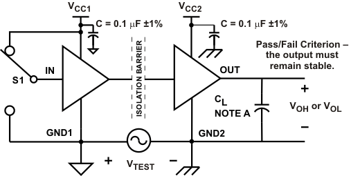
| CMTI |
Common-mode transient immunity |
VI = VCC or 0 V; see Figure 13 |
25 |
75 |
|
kV/μs |
(1) VCCO is the supply voltage, VCC1 or VCC2, for the output channel that is being measured.
6.7 Electrical Characteristics: VCC1 and VCC2 at 3.3 V ±10%
VCC1 and VCC2 at 3.3 V ±10% (over recommended operating conditions unless otherwise noted.)
| PARAMETER |
TEST CONDITIONS |
MIN |
TYP |
MAX |
UNIT |
| VOH |
High-level output voltage |
IOH = –4 mA; see Figure 10 |
VCCO(1) – 0.5 |
3 |
|
V |
| IOH = –20 μA; see Figure 10 |
VCCO(1) – 0.1 |
3.3 |
|
| VOL |
Low-level output voltage |
IOL = 4 mA; see Figure 10 |
|
0.2 |
0.4 |
V |
| IOL = 20 μA; see Figure 10 |
|
0 |
0.1 |
| VI(HYS) |
Input threshold voltage hysteresis |
|
|
425 |
|
mV |
| IIH |
High-level input current |
VIH = VCC at INx or ENx |
|
|
10 |
μA |
| IIL |
Low-level input current |
VIL = 0 V at INx or ENx |
–10 |
|
|
μA |
| CMTI |
Common-mode transient immunity |
VI = VCC or 0 V; see Figure 13 |
25 |
50 |
|
kV/μs |
(1) VCCO is the supply voltage, VCC1 or VCC2, for the output channel that is being measured.
6.8 Electrical Characteristics: VCC1 and VCC2 at 2.7 V
VCC1 and VCC2 at 2.7 V (over recommended operating conditions unless otherwise noted.)
| PARAMETER |
TEST CONDITIONS |
MIN |
TYP |
MAX |
UNIT |
| VOH |
High-level output voltage |
IOH = –2 mA; see Figure 10 |
VCCO(1) – 0.3 |
2.5 |
|
V |
| IOH = –20 μA; see Figure 10 |
VCCO(1) – 0.1 |
2.7 |
|
| VOL |
Low-level output voltage |
IOL = 4 mA; see Figure 10 |
|
0.2 |
0.4 |
V |
| IOL = 20 μA; see Figure 10 |
|
0 |
0.1 |
| VI(HYS) |
Input threshold voltage hysteresis |
|
|
350 |
|
mV |
| IIH |
High-level input current |
VIH = VCC at INx or ENx |
|
|
10 |
μA |
| IIL |
Low-level input current |
VIL = 0 V at INx or ENx |
–10 |
|
|
μA |
| CMTI |
Common-mode transient immunity |
VI = VCC or 0 V; see Figure 13 |
25 |
50 |
|
kV/μs |
(1) VCCO is the supply voltage, VCC1 or VCC2, for the output channel that is being measured.
6.9 Switching Characteristics: VCC1 and VCC2 at 5 V ±10%
VCC1 and VCC2 at 5 V ±10% (over recommended operating conditions unless otherwise noted.)
|
PARAMETER |
TEST CONDITIONS |
MIN |
TYP |
MAX |
UNIT |
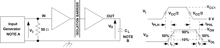
| tPLH, tPHL |
Propagation delay time |
See Figure 10 |
12 |
19 |
35 |
ns |
| PWD(1) |
Pulse width distortion |tPHL – tPLH| |
|
|
3 |
| tsk(o)(2) |
Channel-to-channel output skew time |
Same-direction channels |
|
|
2 |
ns |
| Opposite-direction channels |
|
|
4 |
| tsk(pp)(3) |
Part-to-part skew time |
|
|
|
12 |
ns |
| tr |
Output signal rise time |
See Figure 10 |
|
2 |
|
ns |
| tf |
Output signal fall time |
|
2 |
|
ns |
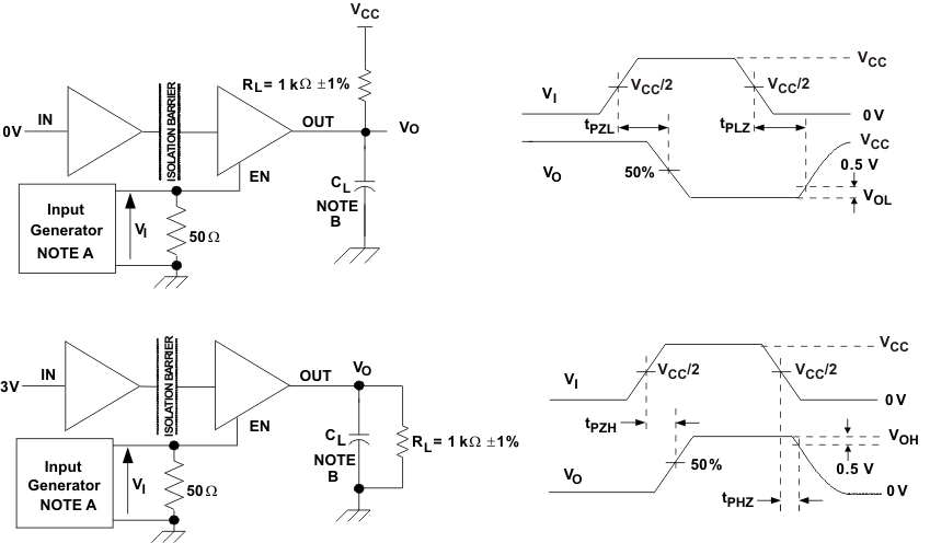
| tPHZ, tPLZ |
Disable propagation delay, high/low-to-high impedance output |
See Figure 11 |
|
6 |
10 |
ns |
| tPZH, tPZL |
Enable propagation delay, high impedance-to-high/low output |
|
5 |
10 |
ns |
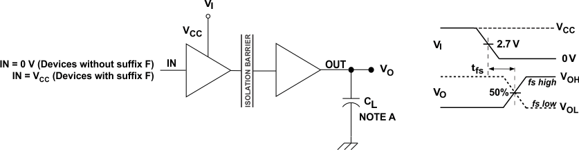
| tfs |
Fail-safe output delay time from input data or power loss |
See Figure 12 |
|
9.5 |
|
μs |
| tGR |
Input glitch rejection time |
|
|
11 |
|
ns |
(1) Also known as pulse skew
(2) tsk(o) is the skew between outputs of a single device with all driving inputs connected together and the outputs switching in the same direction while driving identical loads.
(3) tsk(pp) is the magnitude of the difference in propagation delay times between any terminals of different devices switching in the same direction while operating at identical supply voltages, temperature, input signals, and loads.
6.10 Switching Characteristics: VCC1 and VCC2 at 3.3 V ±10%
VCC1 and VCC2 at 3.3 V ±10% (over recommended operating conditions unless otherwise noted.)
|
PARAMETER |
TEST CONDITIONS |
MIN |
TYP |
MAX |
UNIT |
| tPLH, tPHL |
Propagation delay time |
See Figure 10 |
15 |
23 |
45 |
ns |
| PWD(1) |
Pulse width distortion |tPHL – tPLH| |
|
|
3 |
| tsk(o)(2) |
Channel-to-channel output skew time |
Same-direction Channels |
|
|
2 |
ns |
| Opposite-direction Channels |
|
|
4 |
| tsk(pp)(3) |
Part-to-part skew time |
|
|
|
19 |
ns |
| tr |
Output signal rise time |
See Figure 10 |
|
2.5 |
|
ns |
| tf |
Output signal fall time |
|
2.5 |
|
ns |
| tPHZ, tPLZ |
Disable propagation delay, from high/low to high-impedance output |
See Figure 11 |
|
6.5 |
15 |
ns |
| tPZH, tPZL |
Enable propagation delay, from high-impedance to high/low output |
|
6.5 |
15 |
ns |
| tfs |
Fail-safe output delay time from input data or power loss |
See Figure 12 |
|
8 |
|
μs |
| tGR |
Input glitch rejection time |
|
|
12.5 |
|
ns |
(1) Also known as pulse skew
(2) tsk(o) is the skew between outputs of a single device with all driving inputs connected together and the outputs switching in the same direction while driving identical loads.
(3) tsk(pp) is the magnitude of the difference in propagation delay times between any terminals of different devices switching in the same direction while operating at identical supply voltages, temperature, input signals and loads.
6.11 Switching Characteristics: VCC1 and VCC2 at 2.7 V
VCC1 and VCC2 at 2.7 V (over recommended operating conditions unless otherwise noted.)
|
PARAMETER |
TEST CONDITIONS |
MIN |
TYP |
MAX |
UNIT |
| tPLH, tPHL |
Propagation delay time |
See Figure 10 |
15 |
27 |
50 |
ns |
| PWD(1) |
Pulse width distortion |tPHL – tPLH| |
|
|
3 |
| tsk(o)(2) |
Channel-to-channel output skew time |
Same-direction Channels |
|
|
2 |
ns |
| Opposite-direction Channels |
|
|
4 |
| tsk(pp)(3) |
Part-to-part skew time |
|
|
|
22 |
ns |
| tr |
Output signal rise time |
See Figure 10 |
|
3 |
|
ns |
| tf |
Output signal fall time |
|
3 |
|
ns |
| tPHZ, tPLZ |
Disable propagation delay, from high/low to high-impedance output |
See Figure 11 |
|
9 |
15 |
ns |
| tPZH, tPZL |
Enable propagation delay, from high-impedance to high/low output |
|
9 |
15 |
ns |
| tfs |
Fail-safe output delay time from input data or power loss |
See Figure 12 |
|
8.5 |
|
μs |
| tGR |
Input glitch rejection time |
|
|
14 |
|
ns |
(1) Also known as pulse skew
(2) tsk(o) is the skew between outputs of a single device with all driving inputs connected together and the outputs switching in the same direction while driving identical loads.
(3) tsk(pp) is the magnitude of the difference in propagation delay times between any terminals of different devices switching in the same direction while operating at identical supply voltages, temperature, input signals, and loads.
6.12 Supply Current: VCC1 and VCC2 at 5 V ±10%
VCC1 and VCC2 at 5 V ±10% (over recommended operating conditions unless otherwise noted.)
| PARAMETER |
TEST CONDITIONS |
MIN |
TYP |
MAX |
UNIT |
| ISO7131 |
|
|
|
| ICC1 |
Disable |
EN1 = EN2 = 0 V |
|
2.2 |
3.7 |
mA |
| ICC2 |
|
3.7 |
5 |
| ICC1 |
DC to 1 Mbps |
DC signal: VI = VCC or 0 V
AC signal: All channels switching with square-wave clock input; CL = 15 pF |
|
2.2 |
3.7 |
mA |
| ICC2 |
|
3.7 |
5 |
| ICC1 |
10 Mbps |
|
3.4 |
4.8 |
| ICC2 |
|
4.9 |
6.6 |
| ICC1 |
25 Mbps |
|
4.9 |
6.6 |
| ICC2 |
|
6.8 |
9 |
| ICC1 |
50 Mbps |
|
7.1 |
10 |
| ICC2 |
|
10.5 |
13 |
| ISO7140 |
|
|
|
| ICC1 |
Disable |
EN = 0 V |
|
0.6 |
1.2 |
mA |
| ICC2 |
|
4.6 |
7 |
| ICC1 |
DC to 1 Mbps |
DC Signal: VI = VCC or 0 V,
AC Signal: All channels switching with square wave clock input; CL = 15 pF |
|
0.6 |
1.3 |
mA |
| ICC2 |
|
4.8 |
7 |
| ICC1 |
10 Mbps |
|
1.4 |
2.2 |
| ICC2 |
|
6.9 |
9.2 |
| ICC1 |
25 Mbps |
|
2.7 |
3.9 |
| ICC2 |
|
10.3 |
13.5 |
| ICC1 |
50 Mbps |
|
4.7 |
6.5 |
| ICC2 |
|
15.6 |
21 |
| ISO7141 |
|
|
|
| ICC1 |
Disable |
EN1 = EN2 = 0V |
|
2.5 |
4.2 |
mA |
| ICC2 |
|
4.2 |
7 |
| ICC1 |
DC to 1 Mbps |
DC signal: VI = VCC or 0 V,
AC signal: All channels switching with square wave clock input; CL = 15 pF |
|
2.5 |
4.2 |
mA |
| ICC2 |
|
4.2 |
7 |
| ICC1 |
10 Mbps |
|
3.8 |
5.3 |
| ICC2 |
|
6.2 |
9.6 |
| ICC1 |
25 Mbps |
|
5.6 |
7.5 |
| ICC2 |
|
9.2 |
13 |
| ICC1 |
50 Mbps |
|
8.4 |
11.2 |
| ICC2 |
|
14 |
18.5 |
6.13 Supply Current: VCC1 and VCC2 at 3.3 V ±10%
VCC1 and VCC2 at 3.3 V ±10% (over recommended operating conditions unless otherwise noted.)
| PARAMETER |
TEST CONDITIONS |
MIN |
TYP |
MAX |
UNIT |
| ISO7131 |
|
|
|
| ICC1 |
Disable |
EN1 = EN2 = 0 V |
|
1.9 |
2.7 |
mA |
| ICC2 |
|
2.6 |
3.8 |
| ICC1 |
DC to 1 Mbps |
DC signal: VI = VCC or 0 V
AC signal: All channels switching with square-wave clock input; CL = 15 pF |
|
1.9 |
2.7 |
mA |
| ICC2 |
|
2.6 |
3.8 |
| ICC1 |
10 Mbps |
|
2.4 |
3.5 |
| ICC2 |
|
3.5 |
4.7 |
| ICC1 |
25 Mbps |
|
3.2 |
4.6 |
| ICC2 |
|
4.7 |
6.2 |
| ICC1 |
40 Mbps |
|
5 |
7 |
| ICC2 |
|
7 |
9 |
| ISO7140 |
|
|
|
| ICC1 |
Disable |
EN = 0 V |
|
0.3 |
0.7 |
mA |
| ICC2 |
|
3.6 |
5.2 |
| ICC1 |
DC to 1 Mbps |
DC signal: VI = VCC or 0 V,
AC signal: All channels switching with square-wave clock input; CL = 15 pF |
|
0.4 |
0.8 |
mA |
| ICC2 |
|
3.7 |
5.3 |
| ICC1 |
10 Mbps |
|
0.9 |
1.4 |
| ICC2 |
|
5.1 |
6.8 |
| ICC1 |
25 Mbps |
|
1.7 |
2.4 |
| ICC2 |
|
7.3 |
10 |
| ICC1 |
40 Mbps |
|
2.4 |
3.7 |
| ICC2 |
|
9.4 |
13 |
| ISO7141 |
|
|
|
| ICC1 |
Disable |
EN1 = EN2 = 0 V |
|
2 |
3.1 |
mA |
| ICC2 |
|
3.2 |
4.9 |
| ICC1 |
DC to 1 Mbps |
DC signal: VI = VCC or 0 V,
AC signal: All channels switching with square-wave clock input; CL = 15 pF |
|
2 |
3.1 |
mA |
| ICC2 |
|
3.2 |
4.9 |
| ICC1 |
10 Mbps |
|
2.8 |
3.8 |
| ICC2 |
|
4.5 |
6.1 |
| ICC1 |
25 Mbps |
|
4 |
5.2 |
| ICC2 |
|
6.4 |
8.3 |
| ICC1 |
40 Mbps |
|
5 |
8 |
| ICC2 |
|
8.2 |
11.6 |
6.14 Supply Current: VCC1 and VCC2 at 2.7 V
VCC1 and VCC2 at 2.7 V (over recommended operating conditions unless otherwise noted.)
| PARAMETER |
TEST CONDITIONS |
MIN |
TYP |
MAX |
UNIT |
| ISO7131 |
|
|
|
| ICC1 |
Disable |
EN1 = EN2 = 0 V |
|
1.2 |
2.4 |
mA |
| ICC2 |
|
2.3 |
3.3 |
| ICC1 |
DC to 1 Mbps |
DC signal: VI = VCC or 0 V
AC signal: All channels switching with square-wave clock input; CL = 15 pF |
|
1.2 |
2.4 |
mA |
| ICC2 |
|
2.3 |
3.3 |
| ICC1 |
10 Mbps |
|
2.1 |
3 |
| ICC2 |
|
2.9 |
4 |
| ICC1 |
25 Mbps |
|
3 |
3.8 |
| ICC2 |
|
4 |
5.2 |
| ICC1 |
40 Mbps |
|
4.2 |
5.3 |
| ICC2 |
|
5.8 |
7 |
| ISO7140 |
|
|
|
| ICC1 |
Disable |
EN = 0 V |
|
0.2 |
0.4 |
mA |
| ICC2 |
|
3.2 |
4.7 |
| ICC1 |
DC to 1 Mbps |
DC signal: VI = VCC or 0 V,
AC signal: All channels switching with square-wave clock input; CL = 15 pF |
|
0.2 |
0.5 |
mA |
| ICC2 |
|
3.4 |
4.8 |
| ICC1 |
10 Mbps |
|
0.6 |
1 |
| ICC2 |
|
4.5 |
6.3 |
| ICC1 |
25 Mbps |
|
1.2 |
1.8 |
| ICC2 |
|
6.2 |
8 |
| ICC1 |
40 Mbps |
|
1.8 |
2.6 |
| ICC2 |
|
8 |
11 |
| ISO7141 |
|
|
|
| ICC1 |
Disable |
EN1 = EN2 = 0 V |
|
1.6 |
2.6 |
mA |
| ICC2 |
|
2.8 |
4.1 |
| ICC1 |
DC to 1 Mbps |
DC signal: VI = VCC or 0 V,
AC signal: All channels switching with square-wave clock input; CL = 15 pF |
|
1.6 |
2.6 |
mA |
| ICC2 |
|
2.8 |
4.1 |
| ICC1 |
10 Mbps |
|
2.3 |
3.2 |
| ICC2 |
|
3.8 |
5 |
| ICC1 |
25 Mbps |
|
3.3 |
4.2 |
| ICC2 |
|
5.4 |
6.8 |
| ICC1 |
40 Mbps |
|
4.3 |
5.8 |
| ICC2 |
|
6.9 |
9.2 |
6.15 Typical Characteristics
 Figure 1. ISO7131 Supply Current for All Channels vs Data Rate
 Figure 3. ISO7141 Supply Current for All Channels vs Data Rate
 Figure 5. Low-Level Output Voltage vs Low-Level Output Current
 Figure 7. Propagation Delay Time vs Free-Air Temperature
 Figure 9. Input Glitch Rejection vs Free-Air Temperature
 Figure 2. ISO7140 Supply Current for All Channels vs Data Rate
 Figure 4. High-Level Output Voltage vs High-Level Output Current
 Figure 6. VCC Undervoltage Threshold vs Free-Air Temperature
 Figure 8. Output Jitter vs Data Rate