SLLS629M January 2006 – October 2024 ISO721 , ISO721M , ISO722 , ISO722M
PRODUCTION DATA
- 1
- 1 Features
- 2 Applications
- 3 Description
- 4 Device Comparison Table
- 5 Pin Configuration and Functions
-
6 Specifications
- 6.1 Absolute Maximum Ratings
- 6.2 ESD Ratings
- 6.3 Recommended Operating Conditions
- 6.4 Thermal Information
- 6.5 Power Ratings
- 6.6 Safety Limiting Values
- 6.7 Insulation Specifications
- 6.8 Safety-Related Certifications
- 6.9 Electrical Characteristics, 5 V, 3.3 V
- 6.10 Electrical Characteristics, 5 V
- 6.11 Switching Characteristics, 3.3 V, 5 V
- 6.12 Electrical Characteristics, 3.3 V, 5 V
- 6.13 Electrical Characteristics, 3.3 V
- 6.14 Switching Characteristics, 3.3 V
- 6.15 Switching Characteristics, 5 V, 3.3 V
- 6.16 Switching Characteristics, 5 V
- 6.17 Typical Characteristics
- 7 Parameter Measurement Information
- 8 Detailed Description
- 9 Application and Implementation
- 10Device and Documentation Support
- 11Revision History
- 12Mechanical, Packaging, and Orderable Information
Package Options
Mechanical Data (Package|Pins)
- D|8
Thermal pad, mechanical data (Package|Pins)
Orderable Information
9.2.2 Detailed Design Procedure
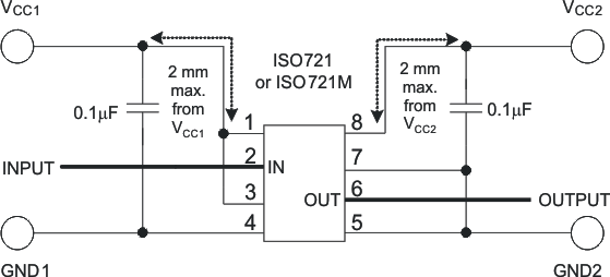
Figure 9-2 shows a typical circuit hook-up for the ISO721 device.
 Figure 9-2 Typical ISO721 Circuit Hook-up
The ISO72x isolators have the same functional pinout as those of most other vendors as shown in Figure 9-3, and are often pin-for-pin drop-in replacements. The notable differences in the products are propagation delay, signaling rate, power consumption, and transient protection rating. Table 9-1 is used as a guide for replacing other isolators with the ISO72x family of single-channel isolators.
 Figure 9-3 Pin Cross Reference
Table 9-1 Cross Reference
| ISOLATOR | PIN 1 | PIN 2 | PIN 3 | PIN 4 | PIN 5 | PIN 6 | PIN 7 | PIN 8 | |
|---|---|---|---|---|---|---|---|---|---|
| ISO721 OR ISO721M | ISO722 OR ISO722M | ||||||||
| ISO721(1)(2) | VCC1 | IN | VCC1 | GND1 | GND2 | OUT | GND2 | EN | VCC2 |
| ADuM1100(1)(2) | VDD1 | VI | VDD1 | GND1 | GND2 | VO | GND2 | VDD2 | |
| HCPL-xxxx | VDD1 | VI | *Leave Open(3) | GND1 | GND2 | VO | NC(5) | VDD2 | |
| IL710 | VDD1 | VI | NC(4) | GND1 | GND2 | VO | V OE | VDD2 | |
(1) Pin 1 must be used as VCC1. Pin 3 can also be used as
VCC1 or left open, as long as pin 1 is connected to
VCC1.
(2) Pin 5 must be used as GND2. Pin 7 can also be used as GND2 or left open, as
long as pin 5 is connected to GND2.
(3) Pin 3 of the HCPL devices must be left open. This is not a problem when substituting an ISO72x device, because the extra VCC1 on pin 3 can be left an open circuit as well.
(4) Pin 3 of the IL710 must not be tied to ground on the circuit board because this shorts the ISO72x VCC1 to ground. The IL710 pin 3 can only be tied to VCC or left open to drop in an ISO72x device.
(5) An HCPL device pin 7 must be left floating (open) or grounded when an ISO722 or ISO722M device is to be used as a drop-in replacement. If pin 7 of the ISO722 or ISO722M device is placed in a high logic state, the output of the device is disabled.