SLLS918D July 2008 – November 2024 ISO721-Q1 , ISO722-Q1
PRODUCTION DATA
- 1
- 1 Features
- 2 Applications
- 3 Description
- 4 Device Comparison Table
- 5 Pin Configuration and Functions
-
6 Specifications
- 6.1 Absolute Maximum Ratings
- 6.2 Recommended Operating Conditions
- 6.3 Thermal Information
- 6.4 Power Ratings
- 6.5 Insulation Specifications
- 6.6 Safety-Related Certifications
- 6.7 Safety Limiting Values
- 6.8 Electrical Characteristics: VCC1 and VCC2 5-V Operation
- 6.9 Electrical Characteristics: VCC1 and VCC2 at 3.3-V Operation
- 6.10 Electrical Characteristics: VCC1 at 3.3-V, VCC2 at 5-V Operation
- 6.11 Electrical Characteristics: VCC1 at 5-V, VCC2 at 3.3-V Operation
- 6.12 Switching Characteristics: VCC1 and VCC2 5-V Operation
- 6.13 Switching Characteristics: VCC1 and VCC2 at 3.3-V Operation
- 6.14 Switching Characteristics: VCC1 at 3.3-V, VCC2 at 5-V Operation
- 6.15 Switching Characteristics: VCC1 at 5-V, VCC2 at 3.3-V Operation
- 6.16 Typical Characteristics
- 6.17 Insulation Characteristics Curves
- 7 Parameter Measurement Information
- 8 Detailed Description
- 9 Application and Implementation
- 10Device and Documentation Support
- 11Revision History
- 12Mechanical, Packaging, and Orderable Information
Package Options
Mechanical Data (Package|Pins)
- D|8
Thermal pad, mechanical data (Package|Pins)
Orderable Information
6.16 Typical Characteristics
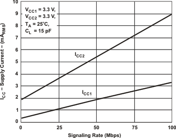 Figure 6-1 RMS Supply Current Versus Signaling
Rate
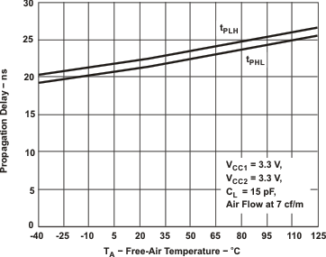 Figure 6-3 Propagation Delay Versus Free-Air
Temperature
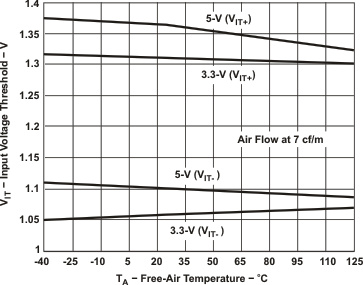 Figure 6-5 Input Threshold Voltage
Versus Free-Air Temperature
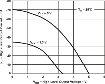 Figure 6-7 High-Level Output Current
Versus High-Level Output Voltage
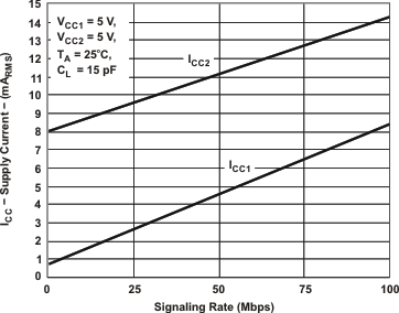 Figure 6-2 RMS Supply Current Versus
Signaling Rate
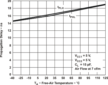 Figure 6-4 Propagation Delay Versus Free-Air
Temperature
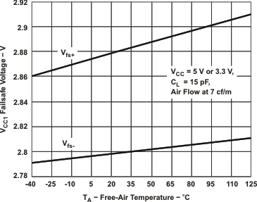 Figure 6-6 VCC1 Failsafe
Threshold Voltage Versus Free-Air Temperature
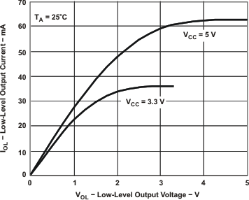 Figure 6-8 Low-Level Output Current
Versus Low-Level Output Voltage