SLLS965E July 2009 – November 2024 ISO7220A-Q1 , ISO7221A-Q1 , ISO7221C-Q1
PRODUCTION DATA
- 1
- 1 Features
- 2 Applications
- 3 Description
- 4 Pin Configuration and Functions
-
5 Specifications
- 5.1 Absolute Maximum Ratings
- 5.2 Recommended Operating Conditions
- 5.3 Safety-Related Certifications
- 5.4 Thermal Information
- 5.5 Safety Limiting Values
- 5.6 Insulation Specifications
- 5.7 Electrical Characterstics
- 5.8 Electrical Characteristics
- 5.9 Electrical Characteristics
- 5.10 Electrical Charcteristics
- 5.11 Switching Characteristics
- 5.12 Switching Characteristics
- 5.13 Switching Characteristics
- 5.14 Switching Characteristics
- 5.15 Typical Characteristics
- 6 Parameter Measurement Information
- 7 Detailed Description
- 8 Application and Implementation
- 9 Device and Documentation Support
- 10Revision History
- 11Mechanical, Packaging, and Orderable Information
Package Options
Mechanical Data (Package|Pins)
- D|8
Thermal pad, mechanical data (Package|Pins)
Orderable Information
3 Description
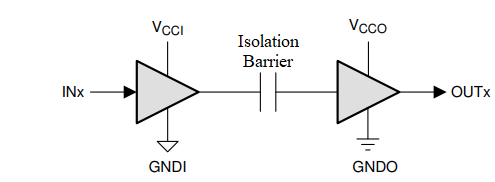
The ISO7220x-Q1 and ISO7221x-Q1 family devices are dual-channel digital isolators. To facilitate PCB layout, the channels are oriented in the same direction in the ISO7220x-Q1 and in opposite directions in the ISO7221x-Q1. These devices have a logic input and output buffer separated by TI’s silicon-dioxide (SiO2) isolation barrier, providing galvanic isolation of up to 4000VPK per VDE. Used in conjunction with isolated power supplies, these devices block high voltage and isolate grounds, as well as prevent noise currents on a data bus or other circuits from entering the local ground and interfering with or damaging sensitive circuitry.
A binary input signal is conditioned, translated to a balanced signal, then differentiated by the capacitive isolation barrier. Across the isolation barrier, a differential comparator receives the logic transition information, then sets or resets a flip-flop and the output circuit accordingly. A periodic update pulse is sent across the barrier to verify that the proper dc level of the output. If this dc-refresh pulse is not received every 4μs, the input is assumed to be unpowered or not being actively driven, and the failsafe circuit drives the output to a logic high state.
The small capacitance and resulting time constant provide fast operation with signaling rates available from 0Mbps (DC) to 25Mbps (The signaling rate of a line is the number of voltage transitions that are made per second expressed in the units bps). The A-option, and C-option devices have TTL input thresholds and a noise filter at the input that prevents transient pulses from being passed to the output of the device. The M-option devices have CMOS VCC/2 input thresholds and do not have the input noise filter and the additional propagation delay.
The ISO7220x-Q1 and ISO7221x-Q1 family of devices require two supply voltages of 2.8V (C-Grade), 3.3V, 5V, or any combination. All inputs are 5V tolerant when supplied from a 2.8V or 3.3V supply and all outputs are 4mA CMOS.
The ISO7220x-Q1 and ISO7221x-Q1 family of devices are characterized for operation over the ambient temperature range of –40°C to +125°C.
| PART NUMBER | PACKAGE(1) | BODY SIZE (NOM) | PACKAGE SIZE(2) |
|---|---|---|---|
| ISO7220x-Q1 | D (SOIC, 8) | 4.90mm × 3.91mm | 4.9mm × 6mm |
| ISO7221x-Q1 |
