SLLS867L September 2007 – October 2024 ISO7230C , ISO7231C , ISO7231M
PRODUCTION DATA
- 1
- 1 Features
- 2 Applications
- 3 Description
- 4 Device Comparison Table
- 5 Pin Configuration and Functions
-
6 Specifications
- 6.1 Absolute Maximum Ratings
- 6.2 ESD Ratings
- 6.3 Thermal Information
- 6.4 Recommended Operating Conditions
- 6.5 Power Ratings
- 6.6 Insulation Specifications
- 6.7 Safety-Related Certifications
- 6.8 Safety Limiting Values
- 6.9 Electrical Characteristics: VCC1 and VCC2 at 3.3 V
- 6.10 Electrical Characteristics: VCC1 and VCC2 at 5-V
- 6.11 Electrical Characteristics: VCC1 at 3.3-V, VCC2 at 5-V
- 6.12 Electrical Characteristics: VCC1 at 5-V, VCC2 at 3.3-V
- 6.13 Switching Characteristics: VCC1 and VCC2 at 3.3-V
- 6.14 Switching Characteristics: VCC1 and VCC2 at 5-V
- 6.15 Switching Characteristics: VCC1 at 3.3-V and VCC2 at 5-V
- 6.16 Switching Characteristics: VCC1 at 5-V, VCC2 at 3.3-V
- 6.17 Typical Characteristics
- 7 Parameter Measurement Information
- 8 Detailed Description
- 9 Application and Implementation
- 10Device and Documentation Support
- 11Revision History
- 12Mechanical, Packaging, and Orderable Information
Package Options
Refer to the PDF data sheet for device specific package drawings
Mechanical Data (Package|Pins)
- DW|16
Thermal pad, mechanical data (Package|Pins)
- DW|16
Orderable Information
3 Description
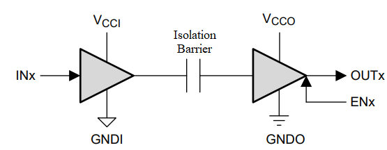
The ISO7230 and ISO7231 are triple-channel digital isolators each with multiple channel configurations and output enable functions. These devices have logic input and output buffers separated by TI’s silicon dioxide (SiO2) isolation barrier. Used in conjunction with isolated power supplies, these devices block high voltage, isolate grounds, and prevent noise currents on a data bus or other circuits from entering the local ground and interfering with or damaging sensitive circuitry.
| PART NUMBER | PACKAGE(1) | BODY SIZE (NOM) | PACKAGE SIZE(2) |
|---|---|---|---|
| ISO7230C ISO7231C ISO7231M |
DW (SOIC, 16) | 10.30mm × 7.50mm | 10.30mm × 10.30mm |
