SLLS867L September 2007 – October 2024 ISO7230C , ISO7231C , ISO7231M
PRODUCTION DATA
- 1
- 1 Features
- 2 Applications
- 3 Description
- 4 Device Comparison Table
- 5 Pin Configuration and Functions
-
6 Specifications
- 6.1 Absolute Maximum Ratings
- 6.2 ESD Ratings
- 6.3 Thermal Information
- 6.4 Recommended Operating Conditions
- 6.5 Power Ratings
- 6.6 Insulation Specifications
- 6.7 Safety-Related Certifications
- 6.8 Safety Limiting Values
- 6.9 Electrical Characteristics: VCC1 and VCC2 at 3.3 V
- 6.10 Electrical Characteristics: VCC1 and VCC2 at 5-V
- 6.11 Electrical Characteristics: VCC1 at 3.3-V, VCC2 at 5-V
- 6.12 Electrical Characteristics: VCC1 at 5-V, VCC2 at 3.3-V
- 6.13 Switching Characteristics: VCC1 and VCC2 at 3.3-V
- 6.14 Switching Characteristics: VCC1 and VCC2 at 5-V
- 6.15 Switching Characteristics: VCC1 at 3.3-V and VCC2 at 5-V
- 6.16 Switching Characteristics: VCC1 at 5-V, VCC2 at 3.3-V
- 6.17 Typical Characteristics
- 7 Parameter Measurement Information
- 8 Detailed Description
- 9 Application and Implementation
- 10Device and Documentation Support
- 11Revision History
- 12Mechanical, Packaging, and Orderable Information
Package Options
Refer to the PDF data sheet for device specific package drawings
Mechanical Data (Package|Pins)
- DW|16
Thermal pad, mechanical data (Package|Pins)
- DW|16
Orderable Information
5 Pin Configuration and Functions
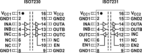
 Figure 5-1 DW Package16-Pin SOICTop View
Table 5-1 Pin Functions
| PIN | TYPE(1) | DESCRIPTION | ||
|---|---|---|---|---|
| NAME | ISO7230 | ISO7231 | ||
| EN | 10 | — | I | Enable, channel A, B, and C |
| EN1 | — | 7 | I | Enable, channel C |
| EN2 | — | 10 | I | Enable, channel A and B |
| GND1 | 2, 8 | 2, 8 | — | Ground connection for VCC1 |
| GND2 | 9, 15 | 9. 15 | — | Ground connection for VCC2 |
| INA | 3 | 3 | I | Input, channel A |
| INB | 4 | 4 | I | Input, channel B |
| INC | 5 | 12 | I | Input, channel C |
| NC | 6, 7, 11 | 6, 11 | — | Not connected |
| OUTA | 14 | 14 | O | Output, channel A |
| OUTB | 13 | 13 | O | Output, channel B |
| OUTC | 12 | 5 | O | Output, channel C |
| VCC1 | 1 | 1 | — | Power supply, VCC1 |
| VCC2 | 16 | 16 | — | Power supply, VCC2 |
(1) I = Input; O = Output