SLLSEU0G November 2016 – October 2024 ISO7740-Q1 , ISO7741-Q1 , ISO7742-Q1
PRODUCTION DATA
- 1
- 1 Features
- 2 Applications
- 3 Description
- 4 Pin Configuration and Functions
-
5 Specifications
- 5.1 Absolute Maximum Ratings
- 5.2 ESD Ratings
- 5.3 Recommended Operating Conditions
- 5.4 Thermal Information
- 5.5 Power Ratings
- 5.6 Insulation Specifications
- 5.7 Safety-Related Certifications
- 5.8 Safety Limiting Values
- 5.9 Electrical Characteristics—5-V Supply
- 5.10 Supply Current Characteristics—5-V Supply
- 5.11 Electrical Characteristics—3.3-V Supply
- 5.12 Supply Current Characteristics—3.3-V Supply
- 5.13 Electrical Characteristics—2.5-V Supply
- 5.14 Supply Current Characteristics—2.5-V Supply
- 5.15 Switching Characteristics—5-V Supply
- 5.16 Switching Characteristics—3.3-V Supply
- 5.17 Switching Characteristics—2.5-V Supply
- 5.18 Insulation Characteristics Curves
- 5.19 Typical Characteristics
- 6 Parameter Measurement Information
- 7 Detailed Description
- 8 Application and Implementation
- 9 Device and Documentation Support
- 10Revision History
- 11Mechanical, Packaging, and Orderable Information
Package Options
Refer to the PDF data sheet for device specific package drawings
Mechanical Data (Package|Pins)
- DBQ|16
- DW|16
Thermal pad, mechanical data (Package|Pins)
- DW|16
Orderable Information
8.2.2 Detailed Design Procedure
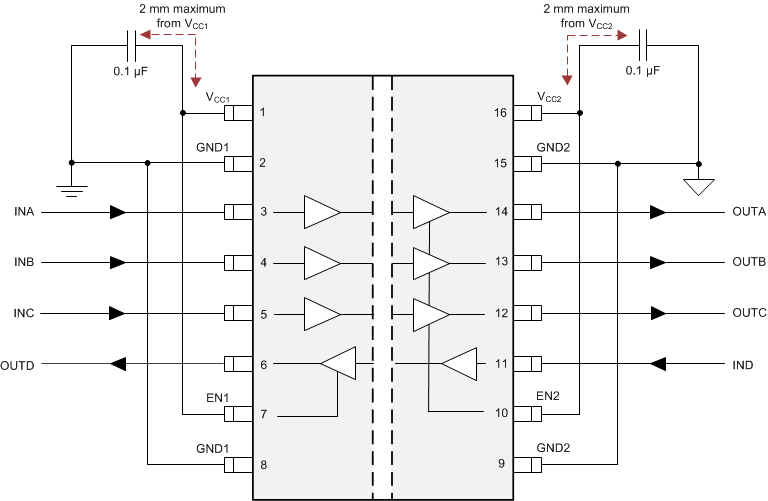
Unlike optocouplers, which require external components to improve performance, provide bias, or limit current, the ISO774x-Q1family of devices only require two external bypass capacitors to operate.
 Figure 8-2 Typical ISO774x-Q1 Circuit Hook-up
The DWW package provides wider creepage and clearance without the need for two isolators in series or an extra isolated power supply, saving design cost and board space. For more details, please refer to the technical document How to Meet the Higher Isolation Creepage & Clearance Needs in Automotive Applications.