SLLSEO2B July   2015  – June 2016 ISO7830

PRODUCTION DATA.  

  1. Features
  2. Applications
  3. Description
  4. Revision History
  5. Pin Configuration and Functions
  6. Specifications
    1. 6.1  Absolute Maximum Ratings
    2. 6.2  ESD Ratings
    3. 6.3  Recommended Operating Conditions
    4. 6.4  Thermal Information
    5. 6.5  Power Rating
    6. 6.6  Insulation Characteristics
    7. 6.7  Regulatory Information
    8. 6.8  Safety Limiting Values
    9. 6.9  Electrical Characteristics—5-V Supply
    10. 6.10 Supply Current Characteristics—5-V Supply
    11. 6.11 Electrical Characteristics—3.3-V Supply
    12. 6.12 Supply Current Characteristics—3.3-V Supply
    13. 6.13 Electrical Characteristics—2.5-V Supply
    14. 6.14 Supply Current Characteristics—2.5-V Supply
    15. 6.15 Switching Characteristics—5-V Supply
    16. 6.16 Switching Characteristics—3.3-V Supply
    17. 6.17 Switching Characteristics—2.5-V Supply
    18. 6.18 Insulation Characteristics Curves
    19. 6.19 Typical Characteristics
  7. Parameter Measurement Information
  8. Detailed Description
    1. 8.1 Overview
    2. 8.2 Functional Block Diagram
    3. 8.3 Feature Description
      1. 8.3.1 Electromagnetic Compatibility (EMC) Considerations
    4. 8.4 Device Functional Modes
      1. 8.4.1 Device I/O Schematics
  9. Application and Implementation
    1. 9.1 Application Information
    2. 9.2 Typical Application
      1. 9.2.1 Design Requirements
      2. 9.2.2 Detailed Design Procedure
      3. 9.2.3 Application Curve
  10. 10Power Supply Recommendations
  11. 11Layout
    1. 11.1 Layout Guidelines
      1. 11.1.1 PCB Material
    2. 11.2 Layout Example
  12. 12Device and Documentation Support
    1. 12.1 Documentation Support
      1. 12.1.1 Related Documentation
    2. 12.2 Related Links
    3. 12.3 Receiving Notification of Documentation Updates
    4. 12.4 Community Resources
    5. 12.5 Trademarks
    6. 12.6 Electrostatic Discharge Caution
    7. 12.7 Glossary
  13. 13Mechanical, Packaging, and Orderable Information

Package Options

Refer to the PDF data sheet for device specific package drawings

Mechanical Data (Package|Pins)
  • DWW|16
  • DW|16
Thermal pad, mechanical data (Package|Pins)
Orderable Information

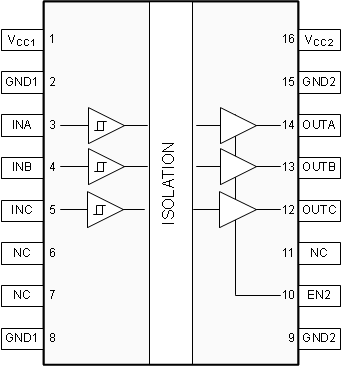
5 Pin Configuration and Functions

DW and DWW Packages
16-Pin SOIC
Top View
ISO7830 ISO7830F po_sllseo2.gif

Pin Functions

PIN I/O DESCRIPTION
NAME NO.
EN2 10 I Output enable 2. Output pins on side 2 are enabled when EN2 is high or open and in high-impedance state when EN2 is low.
GND1 2, 8 Ground connection for VCC1
GND2 9, 15 Ground connection for VCC2
INA 3 I Input, channel A
INB 4 I Input, channel B
INC 5 I Input, channel C
OUTA 14 O Output, channel A
OUTB 13 O Output, channel B
OUTC 12 O Output, channel C
NC 6, 7, 11 Not connected
VCC1 1 Power supply, side 1
VCC2 16 Power supply, side 2