6 Specifications
6.1 Absolute Maximum Ratings
See (1)
| |
MIN |
MAX |
UNIT |
VCC1,
VCC2 |
Supply voltage(2) |
–0.5 |
6 |
V |
|
Voltage |
INx |
–0.5 |
VCCX + 0.5(3) |
V |
| OUTx |
–0.5 |
VCCX + 0.5(3) |
| EN2 |
–0.5 |
VCCX + 0.5(3) |
| IO |
Output current |
–15 |
15 |
mA |
|
Surge immunity |
|
12.8 |
kV |
| Tstg |
Storage temperature |
–65 |
150 |
°C |
(1) Stresses beyond those listed under Absolute Maximum Ratings may cause permanent damage to the device. These are stress ratings only and functional operation of the device at these or any other conditions beyond those indicated under Recommended Operating Conditions is not implied. Exposure to absolute-maximum-rated conditions for extended periods may affect device reliability.
(2) All voltage values except differential I/O bus voltages are with respect to the local ground terminal (GND1 or GND2) and are peak voltage values.
(3) Maximum voltage must not exceed 6 V
6.2 ESD Ratings
|
VALUE |
UNIT |
| V(ESD) |
Electrostatic discharge |
Human body model (HBM), per ANSI/ESDA/JEDEC JS-001, all pins(1) |
±6000 |
V |
| Charged device model (CDM), per JEDEC specification JESD22-C101, all pins(2) |
±1500 |
(1) JEDEC document JEP155 states that 500-V HBM allows safe manufacturing with a standard ESD control process.
(2) JEDEC document JEP157 states that 250-V CDM allows safe manufacturing with a standard ESD control process.
6.3 Recommended Operating Conditions
|
|
MIN |
NOM |
MAX |
UNIT |
| VCC1, VCC2 |
Supply voltage |
2.25 |
|
5.5 |
V |
| IOH |
High-level output current |
VCCO(2) = 5 V |
–4 |
|
|
mA |
| VCCO(2) = 3.3 V |
–2 |
|
|
| VCCO(2) = 2.5 V |
–1 |
|
|
| IOL |
Low-level output current |
VCCO(2) = 5 V |
|
|
4 |
mA |
| VCCO(2) = 3.3 V |
|
|
2 |
| VCCO(2) = 2.5 V |
|
|
1 |
| VIH |
High-level input voltage |
0.7 × VCCI (2) |
|
VCCI (2) |
V |
| VIL |
Low-level input voltage |
0 |
|
0.3 × VCCI(2) |
V |
| DR |
Signaling rate |
0 |
|
100 |
Mbps |
| TJ |
Junction temperature(1) |
–55 |
|
150 |
°C |
| TA |
Ambient temperature |
–55 |
25 |
125 |
°C |
(2) VCCI = Input-side VCC; VCCO = Output-side VCC.
6.4 Thermal Information
|
ISO7840 |
UNIT |
| THERMAL METRIC(1) |
DW (SOIC) |
DWW (SOIC) |
| 16 Pins |
16 Pins |
| RθJA |
Junction-to-ambient thermal resistance |
78.9 |
78.9 |
°C/W |
| RθJC(top) |
Junction-to-case(top) thermal resistance |
41.6 |
41.1 |
°C/W |
| RθJB |
Junction-to-board thermal resistance |
43.6 |
49.5 |
°C/W |
| ψJT |
Junction-to-top characterization parameter |
15.5 |
15.2 |
°C/W |
| ψJB |
Junction-to-board characterization parameter |
43.1 |
48.8 |
°C/W |
| RθJC(bottom) |
Junction-to-case(bottom) thermal resistance |
N/A |
N/A |
°C/W |
6.5 Power Ratings
VCC1 = VCC2 = 5.5 V, TJ = 150°C, CL = 15 pF, input a 50 MHz 50% duty cycle square wave
| PARAMETER |
TEST CONDITIONS |
MIN |
TYP |
MAX |
UNIT |
| PD |
Maximum power dissipation by ISO7840x |
|
|
|
200 |
mW |
| PD1 |
Maximum power dissipation by side-1 of ISO7840x |
|
|
|
40 |
mW |
| PD2 |
Maximum power dissipation by side-2 of ISO7840x |
|
|
|
160 |
mW |
6.6 Insulation Specifications
| PARAMETER |
TEST CONDITIONS |
SPECIFICATION |
UNIT |
| DW |
DWW |
| GENERAL |
| CLR |
External clearance(1) |
Shortest pin-to-pin distance through air |
>8 |
>14.5 |
mm |
| CPG |
External creepage(1) |
Shortest pin-to-pin distance across the package surfaceHigh Voltage Feature Description |
>8 |
>14.5 |
mm |
| DTI |
Distance through the insulation |
Minimum internal gap (internal clearance) |
>21 |
>21 |
μm |
| CTI |
Comparative tracking index |
DIN EN 60112 (VDE 0303-11); IEC 60112; UL 746A |
>600 |
>600 |
V |
|
Material group |
|
I |
I |
|
|
Overvoltage category per IEC 60664-1 |
Rated mains voltage ≤ 600 VRMS |
I–IV |
I–IV |
|
| Rated mains voltage ≤ 1000 VRMS |
I–III |
I–IV |
| DIN V VDE V 0884-10 (VDE V 0884-10):2006-12(2) |
| VIORM |
Maximum repetitive peak isolation voltage |
|
2121 |
2828 |
VPK |
| VIOWM |
Maximum isolation working voltage |
AC voltage (sine wave); Time dependent dielectric breakdown (TDDB) Test, see Figure 1 and Figure 2 |
1500 |
2000 |
VRMS |
| DC voltage |
2121 |
2828 |
VDC |
| VIOTM |
Maximum transient isolation voltage |
VTEST = VIOTM
t = 60 s (qualification)
t= 1 s (100% production) |
8000 |
8000 |
VPK |
| VIOSM |
Maximum surge isolation voltage(3) |
Test method per IEC 60065, 1.2/50 µs waveform,
VTEST = 1.6 × VIOSM = 12800 VPK (qualification) |
8000 |
8000 |
VPK |
| qpd |
Apparent charge(4) |
Method a: After I/O safety test subgroup 2/3,
Vini = VIOTM, tini = 60 s;
Vpd(m) = 1.2 × VIORM = 2545 VPK (DW) and 3394 VPK (DWW), tm = 10 s |
≤5 |
≤5 |
pC |
Method a: After environmental tests subgroup 1,
Vini = VIOTM, tini = 60 s;
Vpd(m) = 1.6 × VIORM = 3394 VPK (DW) and 4525 VPK (DWW), tm = 10 s |
≤5 |
≤5 |
Method b1: At routine test (100% production) and preconditioning (type test)
Vini = VIOTM, tini = 1 s;
Vpd(m) = 1.875 × VIORM = 3977 VPK (DW) and 5303 VPK (DWW), tm = 1 s |
≤5 |
≤5 |
| CIO |
Barrier capacitance, input to output(5) |
VIO = 0.4 × sin (2πft), f = 1 MHz |
2 |
2 |
pF |
| RIO |
Isolation resistance, input to output(5) |
VIO = 500 V, TA = 25°C |
>1012 |
>1012 |
Ω |
| VIO = 500 V, 100°C ≤ TA ≤ 125°C |
>1011 |
>1011 |
| VIO = 500 V at TS = 150°C |
>109 |
>109 |
|
Pollution degree |
|
2 |
2 |
|
|
Climatic category |
|
55/125/21 |
55/125/21 |
|
| UL 1577 |
| VISO |
Withstand isolation voltage |
VTEST = VISO = 5700 VRMS, t = 60 s (qualification),
VTEST = 1.2 × VISO = 6840 VRMS, t = 1 s (100% production) |
5700 |
5700 |
VRMS |
(1) Creepage and clearance requirements should be applied according to the specific equipment isolation standards of an application. Care should be taken to maintain the creepage and clearance distance of a board design to ensure that the mounting pads of the isolator on the printed-circuit board do not reduce this distance. Creepage and clearance on a printed-circuit board become equal in certain cases. Techniques such as inserting grooves, ribs, or both on a printed circuit board are used to help increase these specifications.
(2) This coupler is suitable for safe electrical insulation only within the safety ratings. Compliance with the safety ratings shall be ensured by means of suitable protective circuits.
(3) Testing is carried out in air or oil to determine the intrinsic surge immunity of the isolation barrier.
(4) Apparent charge is electrical discharge caused by a partial discharge (pd).
(5) All pins on each side of the barrier tied together creating a two-pin device.
6.7 Safety-Related Certifications
Certifications for the DW package are complete. DWW package certifications are complete for UL, VDE and TUV and planned for CSA and CQC.
| VDE |
CSA |
UL |
CQC |
TUV |
| Certified according to DIN V VDE V 0884-10 (VDE V 0884-10):2006-12 and DIN EN 60950-1 (VDE 0805 Teil 1):2011-01 |
Approved under CSA Component Acceptance Notice 5A, IEC 60950-1 and IEC 60601-1 |
Certified according to UL 1577 Component Recognition Program |
Certified according to GB 4943.1-2011 |
Certified according to
EN 61010-1:2010 (3rd Ed) and
EN 60950-1:2006/A11:2009/A1:2010/
A12:2011/A2:2013 |
Reinforced insulation
Maximum transient isolation voltage, 8000 VPK;
Maximum repetitive peak isolation voltage, 2121 VPK (DW), 2828 VPK (DWW);
Maximum surge isolation voltage, 8000 VPK |
Reinforced insulation per CSA 60950-1-07+A1+A2 and IEC 60950-1 2nd Ed., 800 VRMS (DW package) and 1450 VRMS (DWW package) max working voltage (pollution degree 2, material group I);
2 MOPP (Means of Patient Protection) per CSA 60601-1:14 and IEC 60601-1 Ed. 3.1, 250 VRMS (354 VPK) max working voltage (DW package) |
Single protection, 5700 VRMS |
Reinforced Insulation, Altitude ≤ 5000 m, Tropical Climate, 250 VRMS maximum working voltage |
5700 VRMS Reinforced insulation per
EN 61010-1:2010 (3rd Ed) up to working voltage of 600 VRMS (DW package) and 1000 VRMS (DWW package)
5700 VRMS Reinforced insulation per
EN 60950-1:2006/A11:2009/A1:2010/
A12:2011/A2:2013 up to working voltage of 800 VRMS (DW package) and 1450 VRMS (DWW package) |
| Certificate number: 40040142 |
Master contract number: 220991 |
File number: E181974 |
Certificate number: CQC15001121716 |
Client ID number: 77311 |
6.8 Safety Limiting Values
Safety limiting intends to minimize potential damage to the isolation barrier upon failure of input or output circuitry. A failure of the I/O can allow low resistance to ground or the supply and, without current limiting, dissipate sufficient power to overheat the die and damage the isolation barrier potentially leading to secondary system failures.
| PARAMETER |
TEST CONDITIONS |
MIN |
TYP |
MAX |
UNIT |
| IS |
Safety input, output, or supply current |
RθJA = 78.9°C/W, VI = 5.5 V, TJ = 150°C, TA = 25°C |
|
|
288 |
mA |
| RθJA = 78.9°C/W, VI = 3.6 V, TJ = 150°C, TA = 25°C |
|
|
440 |
| RθJA = 78.9°C/W, VI = 2.75 V, TJ = 150°C, TA = 25°C |
|
|
576 |
| PS |
Safety input, output, or total power |
RθJA = 78.9°C/W, TJ = 150°C, TA = 25°C |
|
|
1584 |
mW |
| TS |
Maximum safety temperature |
|
|
|
150 |
°C |
The maximum safety temperature is the maximum junction temperature specified for the device. The power dissipation and junction-to-air thermal impedance of the device installed in the application hardware determines the junction temperature. The assumed junction-to-air thermal resistance in the Thermal Information is that of a device installed on a high-K test board for leaded surface-mount packages. The power is the recommended maximum input voltage times the current. The junction temperature is then the ambient temperature plus the power times the junction-to-air thermal resistance.
6.9 Electrical Characteristics—5-V Supply
VCC1 = VCC2 = 5 V ±10% (over recommended operating conditions unless otherwise noted)
| PARAMETER |
TEST CONDITIONS |
MIN |
TYP |
MAX |
UNIT |
| VOH |
High-level output voltage |
IOH = –4 mA; see Figure 11 |
VCCO – 0.4 |
VCCO – 0.2 |
|
V |
| VOL |
Low-level output voltage |
IOL = 4 mA; see Figure 11 |
|
0.2 |
0.4 |
V |
| VI(HYS) |
Input threshold voltage hysteresis |
|
0.1 × VCCI |
|
|
V |
| IIH |
High-level input current |
VIH = VCCI at INx or EN2 |
|
|
10 |
μA |
| IIL |
Low-level input current |
VIL = 0 V at INx or EN2 |
–10 |
|
|
μA |
| CMTI |
Common-mode transient immunity |
VI = VCCI or 0 V, VCM = 1500 V; see Figure 14 |
100 |
|
|
kV/μs |
| CI |
Input capacitance |
VI = VCC/2 + 0.4 × sin (2πft), f = 1 MHz, VCC = 5 V |
|
2 |
|
pF |
6.10 Supply Characteristics—5-V Supply
VCC1 = VCC2 = 5 V ±10% (over recommended operating conditions unless otherwise noted)
| PARAMETER |
TEST CONDITIONS |
SUPPLY CURRENT |
MIN |
TYP |
MAX |
UNIT |
| Supply current |
Disable |
EN2 = 0 V, VI = 0 V (ISO7840F), VI = VCCI(1) (ISO7840) |
ICC1 |
|
1.3 |
2 |
mA |
| ICC2 |
|
0.4 |
0.6 |
| EN2 = 0 V, VI = VCCI (ISO7840F), VI = 0 V (ISO7840) EN2 = 0 V |
ICC1 |
|
6 |
8.5 |
mA |
| ICC2 |
|
0.4 |
0.6 |
| DC signal |
VI = 0 V (ISO7840F), VI = VCCI (ISO7840) |
ICC1 |
|
1.3 |
2 |
mA |
| ICC2 |
|
2.2 |
3.1 |
| VI = VCCI (ISO7840F), VI = 0 V (ISO7840) |
ICC1 |
|
5.9 |
8.6 |
mA |
| ICC2 |
|
2.5 |
3.3 |
| All channels switching with square wave clock input; CL = 15 pF |
1 Mbps |
ICC1 |
|
3.6 |
5.3 |
mA |
| ICC2 |
|
2.6 |
3.7 |
| 10 Mbps |
ICC1 |
|
3.8 |
5.4 |
mA |
| ICC2 |
|
4.5 |
5.9 |
| 100 Mbps |
DW package |
ICC1 |
|
5.1 |
5.9 |
mA |
| ICC2 |
|
23.8 |
27.4 |
| DWW package |
ICC1 |
|
5.1 |
5.9 |
mA |
| ICC2 |
|
23.8 |
28.5 |
(1) VCCI = Input-side VCC; VCCO = Output-side VCC.
6.11 Electrical Characteristics—3.3-V Supply
VCC1 = VCC2 = 3.3 V ±10% (over recommended operating conditions unless otherwise noted)
| PARAMETER |
TEST CONDITIONS |
MIN |
TYP |
MAX |
UNIT |
| VOH |
High-level output voltage |
IOH = –2 mA; see Figure 11 |
VCCO – 0.4 |
VCCO – 0.2 |
|
V |
| VOL |
Low-level output voltage |
IOL = 2 mA; see Figure 11 |
|
0.2 |
0.4 |
V |
| VI(HYS) |
Input threshold voltage hysteresis |
|
0.1 × VCCI |
|
|
V |
| IIH |
High-level input current |
VIH = VCCI at INx or EN2 |
|
|
10 |
μA |
| IIL |
Low-level input current |
VIL = 0 V at INx or EN2 |
–10 |
|
|
μA |
| CMTI |
Common-mode transient immunity |
VI = VCCI or 0 V, VCM = 1500 V; see Figure 14 |
100 |
|
|
kV/μs |
6.12 Supply Current Characteristics—3.3-V Supply
VCC1 = VCC2 = 3.3 V ±10% (over recommended operating conditions unless otherwise noted)
| PARAMETER |
TEST CONDITIONS |
SUPPLY CURRENT |
MIN |
TYP |
MAX |
UNIT |
| Supply current |
Disable |
EN2 = 0 V, VI = 0 V (ISO7840F), VI = VCCI(1) (ISO7840) |
ICC1 |
|
1.3 |
2 |
mA |
| ICC2 |
|
0.4 |
0.6 |
| EN2 = 0 V, VI = VCCI(1) (ISO7840F), VI = 0 V (ISO7840) |
ICC1 |
|
6 |
8.5 |
mA |
| ICC2 |
|
0.4 |
0.6 |
| DC signal |
VI = 0 V (ISO7840F), VI = VCCI(1) (ISO7840) |
ICC1 |
|
1.3 |
2 |
mA |
| ICC2 |
|
2.2 |
3 |
| VI = VCCI(1) (ISO7840F), VI = 0 V (ISO7840) |
ICC1 |
|
5.9 |
8.6 |
mA |
| ICC2 |
|
2.4 |
3.3 |
| All channels switching with square wave clock input; CL = 15 pF |
1 Mbps |
ICC1 |
|
3.6 |
5.3 |
mA |
| ICC2 |
|
2.5 |
3.6 |
| 10 Mbps |
ICC1 |
|
3.7 |
5.3 |
mA |
| ICC2 |
|
3.9 |
5.1 |
| 100 Mbps |
ICC1 |
|
4.5 |
5.8 |
mA |
| ICC2 |
|
17.7 |
20.6 |
(1) VCCI = Input-side VCC; VCCO = Output-side VCC.
6.13 Electrical Characteristics—2.5-V Supply
VCC1 = VCC2 = 2.5 V ±10% (over recommended operating conditions unless otherwise noted)
| PARAMETER |
TEST CONDITIONS |
MIN |
TYP |
MAX |
UNIT |
| VOH |
High-level output voltage |
IOH = –1 mA; see Figure 11 |
VCCO – 0.4 |
VCCO – 0.2 |
|
V |
| VOL |
Low-level output voltage |
IOL = 1 mA; see Figure 11 |
|
0.2 |
0.4 |
V |
| VI(HYS) |
Input threshold voltage hysteresis |
|
0.1 × VCCI |
|
|
V |
| IIH |
High-level input current |
VIH = VCCI at INx or EN2 |
|
|
10 |
μA |
| IIL |
Low-level input current |
VIL = 0 V at INx or EN2 |
–10 |
|
|
μA |
| CMTI |
Common-mode transient immunity |
VI = VCCI or 0 V, VCM = 1500 V; see Figure 14 |
100 |
|
|
kV/μs |
6.14 Supply Current Characteristics—2.5-V Supply
VCC1 = VCC2 = 2.5 V ±10% (over recommended operating conditions unless otherwise noted)
| PARAMETER |
TEST CONDITIONS |
SUPPLY CURRENT |
MIN |
TYP |
MAX |
UNIT |
| Supply current |
Disable |
EN2 = 0 V, VI = 0 V (Devices with suffix F), VI = VCCI(1) (Devices without suffix F) |
ICC1 |
|
1.3 |
2 |
mA |
| ICC2 |
|
0.4 |
0.6 |
| EN2 = 0 V, VI = VCCI(1) (Devices with suffix F), VI = 0 V (Devices without suffix F) |
ICC1 |
|
6 |
8.5 |
mA |
| ICC2 |
|
0.4 |
0.6 |
| DC signal |
VI = 0 V (Devices with suffix F), VI = VCCI(1) (Devices without suffix F) |
ICC1 |
|
1.3 |
2 |
mA |
| ICC2 |
|
2.2 |
3 |
| VI = VCCI(1) (Devices with suffix F), VI = 0 V (Devices without suffix F) |
ICC1 |
|
5.9 |
8.6 |
mA |
| ICC2 |
|
2.4 |
3.3 |
All channels switching with square wave clock input;
CL = 15 pF |
1 Mbps |
ICC1 |
|
3.6 |
5.3 |
mA |
| ICC2 |
|
2.5 |
3.5 |
| 10 Mbps |
ICC1 |
|
3.7 |
5.3 |
mA |
| ICC2 |
|
3.5 |
4.7 |
| 100 Mbps |
ICC1 |
|
4.4 |
5.7 |
mA |
| ICC2 |
|
13.9 |
16.4 |
(1) VCCI = Input-side VCC; VCCO = Output-side VCC.
6.15 Switching Characteristics—5-V Supply
VCC1 = VCC2 = 5 V ±10% (over recommended operating conditions unless otherwise noted)
| PARAMETER |
TEST CONDITIONS |
MIN |
TYP |
MAX |
UNIT |
| tPLH, tPHL |
Propagation delay time |
See Figure 11 |
6 |
11 |
16 |
ns |
| PWD |
Pulse width distortion(1) |tPHL – tPLH| |
|
0.55 |
4.1 |
ns |
| tsk(o) |
Channel-to-channel output skew time(2) |
Same-direction channels |
|
|
2.5 |
ns |
| tsk(pp) |
Part-to-part skew time(3) |
|
|
|
4.5 |
ns |
| tr |
Output signal rise time |
See Figure 11 |
|
1.7 |
3.9 |
ns |
| tf |
Output signal fall time |
|
1.9 |
3.9 |
ns |
| tPHZ |
Disable propagation delay, high-to-high impedance output |
See Figure 12 |
|
12 |
20 |
ns |
| tPLZ |
Disable propagation delay, low-to-high impedance output |
|
12 |
20 |
ns |
| tPZH |
Enable propagation delay, high impedance-to-high output for ISO7840 |
|
10 |
20 |
ns |
| Enable propagation delay, high impedance-to-high output for ISO7840F |
|
2 |
2.5 |
μs |
| tPZL |
Enable propagation delay, high impedance-to-low output for ISO7840 |
|
2 |
2.5 |
μs |
| Enable propagation delay, high impedance-to-low output for ISO7840F |
|
10 |
20 |
ns |
| tfs |
Default output delay time from input power loss |
Measured from the time VCC goes below 1.7 V. See Figure 13 |
|
0.2 |
9 |
μs |
| tie |
Time interval error |
216 – 1 PRBS data at 100 Mbps |
|
0.90 |
|
ns |
(1) Also known as pulse skew.
(2) tsk(o) is the skew between outputs of a single device with all driving inputs connected together and the outputs switching in the same direction while driving identical loads.
(3) tsk(pp) is the magnitude of the difference in propagation delay times between any terminals of different devices switching in the same direction while operating at identical supply voltages, temperature, input signals and loads.
6.16 Switching Characteristics—3.3-V Supply
VCC1 = VCC2 = 3.3 V ±10% (over recommended operating conditions unless otherwise noted)
| PARAMETER |
TEST CONDITIONS |
MIN |
TYP |
MAX |
UNIT |
| tPLH, tPHL |
Propagation delay time |
See Figure 11 |
6 |
10.8 |
16 |
ns |
| PWD |
Pulse width distortion(1) |tPHL – tPLH| |
|
0.7 |
4.2 |
ns |
| tsk(o) |
Channel-to-channel output skew time(2) |
Same-direction channels |
|
|
2.2 |
ns |
| tsk(pp) |
Part-to-part skew time(3) |
|
|
|
4.5 |
ns |
| tr |
Output signal rise time |
See Figure 11 |
|
0.8 |
3 |
ns |
| tf |
Output signal fall time |
|
0.8 |
3 |
ns |
| tPHZ |
Disable propagation delay, high-to-high impedance output |
See Figure 12 |
|
17 |
32 |
ns |
| tPLZ |
Disable propagation delay, low-to-high impedance output |
|
17 |
32 |
ns |
| tPZH |
Enable propagation delay, high impedance-to-high output for ISO7840 |
|
17 |
32 |
ns |
| Enable propagation delay, high impedance-to-high output for ISO7840F |
|
2 |
2.5 |
μs |
| tPZL |
Enable propagation delay, high impedance-to-low output for ISO7840 |
|
2 |
2.5 |
μs |
| Enable propagation delay, high impedance-to-low output for ISO7840F |
|
17 |
32 |
ns |
| tfs |
Default output delay time from input power loss |
Measured from the time VCC goes below 1.7 V. See Figure 13 |
|
0.2 |
9 |
μs |
| tie |
Time interval error |
216 – 1 PRBS data at 100 Mbps |
|
0.91 |
|
ns |
(1) Also known as Pulse Skew.
(2) tsk(o) is the skew between outputs of a single device with all driving inputs connected together and the outputs switching in the same direction while driving identical loads.
(3) tsk(pp) is the magnitude of the difference in propagation delay times between any terminals of different devices switching in the same direction while operating at identical supply voltages, temperature, input signals and loads.
6.17 Switching Characteristics—2.5-V Supply
VCC1 = VCC2 = 2.5 V ±10% (over recommended operating conditions unless otherwise noted)
| PARAMETER |
TEST CONDITIONS |
MIN |
TYP |
MAX |
UNIT |
| tPLH, tPHL |
Propagation delay time |
See Figure 11 |
7.5 |
11.7 |
17.5 |
ns |
| PWD |
Pulse width distortion(1) |tPHL – tPLH| |
|
0.66 |
4.2 |
ns |
| tsk(o) |
Channel-to-channel output skew time(2) |
Same-direction Channels |
|
|
2.2 |
ns |
| tsk(pp) |
Part-to-part skew time(3) |
|
|
|
4.5 |
ns |
| tr |
Output signal rise time |
See Figure 11 |
|
1 |
3.5 |
ns |
| tf |
Output signal fall time |
|
1.2 |
3.5 |
ns |
| tPHZ |
Disable propagation delay, high-to-high impedance output |
See Figure 12 |
|
22 |
45 |
ns |
| tPLZ |
Disable propagation delay, low-to-high impedance output |
|
22 |
45 |
ns |
| tPZH |
Enable propagation delay, high impedance-to-high output for ISO7840 |
|
18 |
45 |
ns |
| Enable propagation delay, high impedance-to-high output for ISO7840F |
|
2 |
2.5 |
μs |
| tPZL |
Enable propagation delay, high impedance-to-low output for ISO7840 |
|
2 |
2.5 |
μs |
| Enable propagation delay, high impedance-to-low output for ISO7840F |
|
18 |
45 |
ns |
| tfs |
Default output delay time from input power loss |
Measured from the time VCC goes below 1.7 V. See Figure 13 |
|
0.2 |
9 |
μs |
| tie |
Time interval error |
216 – 1 PRBS data at 100 Mbps |
|
0.91 |
|
ns |
(1) Also known as pulse skew.
(2) tsk(o) is the skew between outputs of a single device with all driving inputs connected together and the outputs switching in the same direction while driving identical loads.
(3) tsk(pp) is the magnitude of the difference in propagation delay times between any terminals of different devices switching in the same direction while operating at identical supply voltages, temperature, input signals and loads.
6.18 Insulation Characteristics Curves

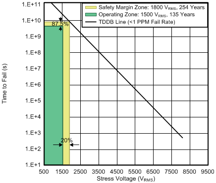
| TA upto 150°C |
Operating lifetime = 135 years |
| Stress-voltage frequency = 60 Hz |
| Isolation working voltage = 1500 VRMS |
Figure 1. Reinforced Isolation Capacitor Life Time Projection for Devices in DW Package
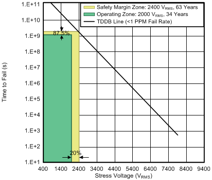
| TA upto 150°C |
Operating lifetime = 34 years |
| Stress-voltage frequency = 60 Hz |
| Isolation working voltage = 2000 VRMS |
Figure 2. Reinforced Isolation Capacitor Life Time Projection for Devices in DWW Package
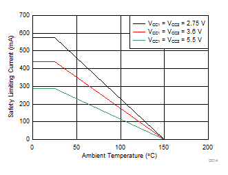 Figure 3. Thermal Derating Curve for Limiting Current per VDE
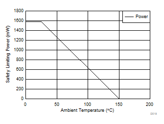 Figure 4. Thermal Derating Curve for Limiting Power per VDE
6.19 Typical Characteristics
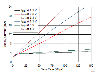
 Figure 5. Supply Current vs Data Rate (With 15-pF Load)
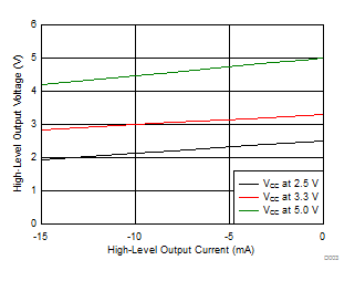
 Figure 7. High-Level Output Voltage vs High-level Output Current
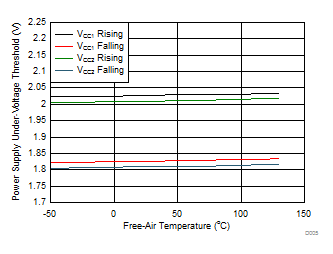
 Figure 9. Power Supply Undervoltage Threshold vs Free-Air Temperature
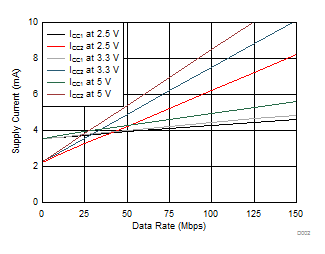
 Figure 6. Supply Current vs Data Rate (With No Load)
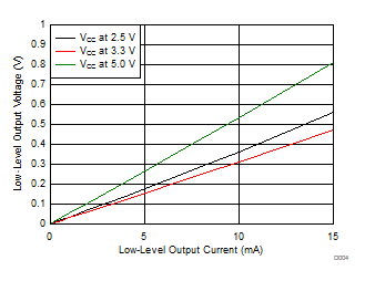
 Figure 8. Low-Level Output Voltage vs Low-Level Output Current
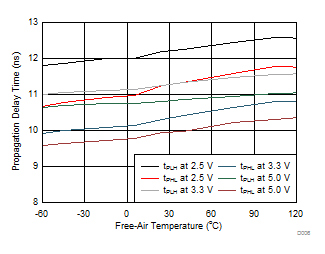
 Figure 10. Propagation Delay Time vs Free-Air Temperature

 Figure 3. Thermal Derating Curve for Limiting Current per VDE
 Figure 4. Thermal Derating Curve for Limiting Power per VDE
