SLLSEJ0H October 2014 – March 2024 ISO7842
PRODUCTION DATA
- 1
- 1 Features
- 2 Applications
- 3 Description
- 4 Pin Configuration and Functions
-
5 Specifications
- 5.1 Absolute Maximum Ratings
- 5.2 ESD Ratings
- 5.3 Recommended Operating Conditions
- 5.4 Thermal Information
- 5.5 Power Ratings
- 5.6 Insulation Specifications
- 5.7 Safety-Related Certifications
- 5.8 Safety Limiting Values
- 5.9 Electrical Characteristics–5V Supply
- 5.10 Supply Current Characteristics–5V Supply
- 5.11 Electrical Characteristics—3.3V Supply
- 5.12 Supply Current Characteristics—3.3V Supply
- 5.13 Electrical Characteristics—2.5V Supply
- 5.14 Supply Current Characteristics—2.5V Supply
- 5.15 Switching Characteristics—5V Supply
- 5.16 Switching Characteristics—3.3V Supply
- 5.17 Switching Characteristics—2.5V Supply
- 5.18 Insulation Characteristics Curves
- 5.19 Typical Characteristics
- Parameter Measurement Information
- 6 Detailed Description
- 7 Application and Implementation
- 8 Power Supply Recommendations
- 9 Layout
- 10Device and Documentation Support
- 11Revision History
- 12Mechanical, Packaging, and Orderable Information
Package Options
Refer to the PDF data sheet for device specific package drawings
Mechanical Data (Package|Pins)
- DWW|16
- DW|16
Thermal pad, mechanical data (Package|Pins)
Orderable Information
3 Description
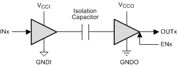
The ISO7842x device is a high-performance, quad-channel digital isolator with a 8000VPK isolation voltage. This device has reinforced isolation certifications according to VDE, CSA, CQC, and TUV. The isolator provides high electromagnetic immunity and low emissions at low-power consumption while isolating CMOS or LVCMOS digital I/Os. Each isolation channel has a logic input and output buffer separated by a silicon-dioxide (SiO2) insulation barrier.
This device comes with enable pins that can be used to put the respective outputs in high impedance for multi-master driving applications and to reduce power consumption. The ISO7842 device has two forward and two reverse-direction channels. If the input power or signal is lost, the default output is high for the ISO7842 device and low for the ISO7842F device. See the Device Functional Modes section for further details.
Used in conjunction with isolated power supplies, this device helps prevent noise currents on a data bus or other circuits from entering the local ground and interfering with or damaging sensitive circuitry. Through innovative chip design and layout techniques, electromagnetic compatibility of the ISO7842 device has been significantly enhanced to ease system-level ESD, EFT, surge, and emissions compliance.
The ISO7842 device is available in 16-pin SOIC wide-body (DW) and extra-wide body (DWW) packages.
| PART NUMBER | PACKAGE(1) | PACKAGE SIZE(2) | BODY SIZE (NOM) |
|---|---|---|---|
| ISO7842 ISO7842F |
DW (16) | 10.30mm × 10.30mm | 10.30mm × 7.50mm |
| DWW (16) | 10.30mm × 17.25mm | 10.30mm × 14.0mm |
