SLLSFW6 March 2024 ISOUSB211-Q1
ADVANCE INFORMATION
- 1
- 1 Features
- 2 Applications
- 3 Description
- 4 Pin Configuration and Functions
-
5 Specifications
- 5.1 Absolute Maximum Ratings
- 5.2 ESD Ratings
- 5.3 Recommended Operating Conditions
- 5.4 Thermal Information
- 5.5 Power Ratings
- 5.6 Insulation Specifications
- 5.7 Safety-Related Certifications
- 5.8 Safety Limiting Values
- 5.9 Electrical Characteristics
- 5.10 Switching Characteristics
- 5.11 Insulation Characteristics Curves
- 5.12 Typical Characteristics
- 6 Parameter Measurement Information
-
7 Detailed Description
- 7.1 Overview
- 7.2 Functional Block Diagram
- 7.3
Feature Description
- 7.3.1 Power Supply Options
- 7.3.2 Power Up
- 7.3.3 Symmetric Operation, Dual-Role Port and Role-Reversal
- 7.3.4 Connect and Speed Detection
- 7.3.5 Disconnect Detection
- 7.3.6 Reset
- 7.3.7 LS/FS Message Traffic
- 7.3.8 HS Message Traffic
- 7.3.9 Equalization and Pre-emphasis
- 7.3.10 L2 Power Management State (Suspend) and Resume
- 7.3.11 L1 Power Management State (Sleep) and Resume
- 7.3.12 HS Test Mode Support
- 7.3.13 CDP Advertising
- 7.4 Device Functional Modes
- 8 Application and Implementation
- 9 Device and Documentation Support
- 10Revision History
- 11Mechanical, Packaging, and Orderable Information
Package Options
Mechanical Data (Package|Pins)
- DP|28
Thermal pad, mechanical data (Package|Pins)
Orderable Information
8.1.1 Isolated Host or Hub
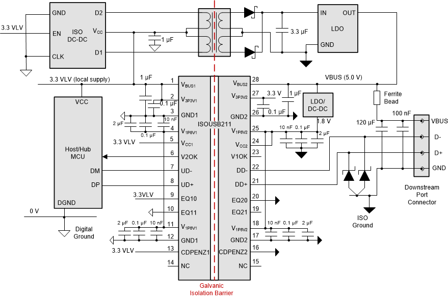
Figure 8-1 shows an application for isolating a host or a hub using ISOUSB211-Q1. In this example, on the microntroller side, V3P3V1 and VBUS1 are together connected to an external 3.3-V supply. The V1P8V1 supply is generated using the internal 1.8-V LDO by providing 3.3-V supply to VCC1. On the connector side, the VBUS from the USB connector is connected to VBUS2 and the V3P3V2 supply is generated using the internal 3.3-V LDO. VCC2 and V1P8V2 are together connected to an external 1.8-V supply derived from VBUS. Please refer to Thermal ConsiderationsThermal ConsiderationsVBUS / V3P3V PowerVCCx / V1P8Vx PowerExample Configuration 1Example Configuration 2Example Configuration 3Example Configuration 3 for options on optimizing power dissipation inside ISOUSB211-Q1 as required.
Decoupling capacitors are placed next to ISOUSB211-Q1 according to the recommendations provided in the Power Supply Recommendations section. An isolated DC-DC converter (such as the SN6505) is to provide power to the VBUS using the 3.3-V local supply. Note that, for a host or hub, the USB standard requires a 120-μF capacitor to be placed on the VBUS so as to be able provide in-rush current when a downstream peripheral is attached. In addition, a 100-nF capacitor is recommended close to the VBUS pin to handle tranisent currents.
ESD diodes with low capacitance and low dynamic resistance, such as PESD5V0C1USF, may be placed on D+ and D- lines. A ferrite bead, with dc resistance less than 100 mΩ, may be optionally placed between VBUS pin of the connector and the VBUS pin of ISOUSB211-Q1, as shown in the figure, to suppress transients such as ESD.
If the isolated power supply used is capable of providing >1.5 A current on the VBUS, the port can be configured as a CDP port according to Battery Charger specification BC 1.2. To do this, the CDPENZ2 pin of ISOUSB211-Q1 must be connected to ground as shown. Under this condition ISOUSB211-Q1 responds to BC 1.2 signaling from a connected peripheral indicating to the peripheral that the port is capable of supply 1.5-A current on VBUS.
 Figure 8-1 Isolated Host or Hub with ISOUSB211-Q1