SLLSFW6 March 2024 ISOUSB211-Q1
ADVANCE INFORMATION
- 1
- 1 Features
- 2 Applications
- 3 Description
- 4 Pin Configuration and Functions
-
5 Specifications
- 5.1 Absolute Maximum Ratings
- 5.2 ESD Ratings
- 5.3 Recommended Operating Conditions
- 5.4 Thermal Information
- 5.5 Power Ratings
- 5.6 Insulation Specifications
- 5.7 Safety-Related Certifications
- 5.8 Safety Limiting Values
- 5.9 Electrical Characteristics
- 5.10 Switching Characteristics
- 5.11 Insulation Characteristics Curves
- 5.12 Typical Characteristics
- 6 Parameter Measurement Information
-
7 Detailed Description
- 7.1 Overview
- 7.2 Functional Block Diagram
- 7.3
Feature Description
- 7.3.1 Power Supply Options
- 7.3.2 Power Up
- 7.3.3 Symmetric Operation, Dual-Role Port and Role-Reversal
- 7.3.4 Connect and Speed Detection
- 7.3.5 Disconnect Detection
- 7.3.6 Reset
- 7.3.7 LS/FS Message Traffic
- 7.3.8 HS Message Traffic
- 7.3.9 Equalization and Pre-emphasis
- 7.3.10 L2 Power Management State (Suspend) and Resume
- 7.3.11 L1 Power Management State (Sleep) and Resume
- 7.3.12 HS Test Mode Support
- 7.3.13 CDP Advertising
- 7.4 Device Functional Modes
- 8 Application and Implementation
- 9 Device and Documentation Support
- 10Revision History
- 11Mechanical, Packaging, and Orderable Information
Package Options
Mechanical Data (Package|Pins)
- DP|28
Thermal pad, mechanical data (Package|Pins)
Orderable Information
8.5.1.1 Layout Example
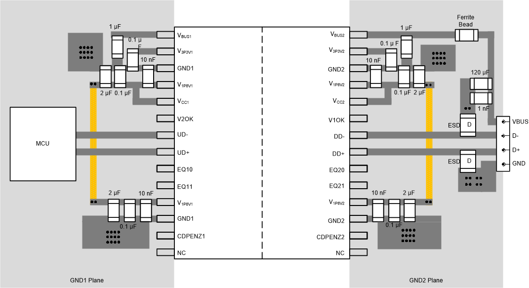
The layout example in this section shows the recommended placement for de-coupling capacitors and ESD protection diodes. A continuous ground plane is recommended below the D+/D- signal traces. Small footprint capacitors (0402/0201) are recommended so that these may be placed very close to the supply pins and corresponding ground pins and connected using the top layer. There should not be any vias in the routing path between the decoupling capacitors and the corresponding supply and ground pins. The capacitors on V1P8Vx supplies are higher in priority when considering placement close to the IC. The ESD protection diodes should be placed close to the connector with a strong connection to the ground plane. Pins 4 and 11 for V1P8V1 and pins 18 and 25 for V1P8V2 are connected together, but this connection is after the de-coupling capacitors. If more than 2 layers are available in the PCB, this connection should be made in an inner or bottom layer (ex. Layer 3 or 4) so as to not interrupt the ground plane under the D+/D- traces. The example shown is for an isolated host or hub, but similar considerations apply for isolated peripherals also. The 120-μF capacitor on VBUS only applies to host or hub and should not be used for peripherals. A ferrite bead, with dc resistance less than 100 mΩ, may be optionally placed on the VBUS route, after the 100-nF (and 120-μF) capacitors to prevent transients such as ESD from affecting the rest of the circuits.  Figure 8-9 Layout Example for ISOUSB211-Q1.
For best performance, it is recommended to minimize the length of D+/D- board traces from the MCU to ISOUSB211-Q1, and from ISOUSB211-Q1 to the connector. Vias and stubs on D+/D- lines must be avoided. This is especially important for High Speed Operation.
Connect a small plane (for example, 2 mm x 2 mm) to the GND pins on the top layer to improve thermal performance. Connect this to the ground player in the second layer with multiple vias.
 Figure 8-9 Layout Example for ISOUSB211-Q1.