SLLSFG1B February 2020 – December 2020 ISOW7841A-Q1
PRODUCTION DATA
- 1 Features
- 2 Applications
- 3 Description
- 4 Revision History
- 5 Description Continued
- 6 Pin Configuration and Functions
-
7 Specifications
- 7.1 Absolute Maximum Ratings
- 7.2 ESD Ratings
- 7.3 Recommended Operating Conditions
- 7.4 Thermal Information
- 7.5 Power Ratings
- 7.6 Insulation Specifications
- 7.7 Safety-Related Certifications
- 7.8 Safety Limiting Values
- 7.9 Electrical Characteristics—5-V Input, 5-V Output
- 7.10 Supply Current Characteristics—5-V Input, 5-V Output
- 7.11 Electrical Characteristics—3.3-V Input, 5-V Output
- 7.12 Supply Current Characteristics—3.3-V Input, 5-V Output
- 7.13 Electrical Characteristics—5-V Input, 3.3-V Output
- 7.14 Supply Current Characteristics—5-V Input, 3.3-V Output
- 7.15 Electrical Characteristics—3.3-V Input, 3.3-V Output
- 7.16 Supply Current Characteristics—3.3-V Input, 3.3-V Output
- 7.17 Switching Characteristics—5-V Input, 5-V Output
- 7.18 Switching Characteristics—3.3-V Input, 5-V Output
- 7.19 Switching Characteristics—5-V Input, 3.3-V Output
- 7.20 Switching Characteristics—3.3-V Input, 3.3-V Output
- 7.21 Insulation Characteristics Curves
- 7.22 Typical Characteristics
- 8 Parameter Measurement Information
- 9 Detailed Description
- 10Application and Implementation
- 11Layout
- 12Device and Documentation Support
- 13Mechanical, Packaging, and Orderable Information
Package Options
Mechanical Data (Package|Pins)
- DWE|16
Thermal pad, mechanical data (Package|Pins)
Orderable Information
7.21 Insulation Characteristics Curves
 Figure 7-1 Thermal Derating Curve for Safety
Limiting Current per VDE
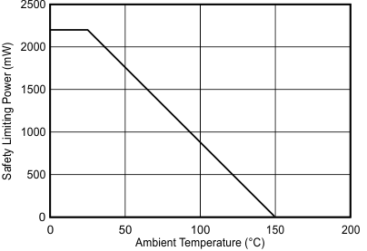
 Figure 7-2 Thermal Derating Curve for Safety
Limiting Power per VDE