SLLSFG1B February 2020 – December 2020 ISOW7841A-Q1
PRODUCTION DATA
- 1 Features
- 2 Applications
- 3 Description
- 4 Revision History
- 5 Description Continued
- 6 Pin Configuration and Functions
-
7 Specifications
- 7.1 Absolute Maximum Ratings
- 7.2 ESD Ratings
- 7.3 Recommended Operating Conditions
- 7.4 Thermal Information
- 7.5 Power Ratings
- 7.6 Insulation Specifications
- 7.7 Safety-Related Certifications
- 7.8 Safety Limiting Values
- 7.9 Electrical Characteristics—5-V Input, 5-V Output
- 7.10 Supply Current Characteristics—5-V Input, 5-V Output
- 7.11 Electrical Characteristics—3.3-V Input, 5-V Output
- 7.12 Supply Current Characteristics—3.3-V Input, 5-V Output
- 7.13 Electrical Characteristics—5-V Input, 3.3-V Output
- 7.14 Supply Current Characteristics—5-V Input, 3.3-V Output
- 7.15 Electrical Characteristics—3.3-V Input, 3.3-V Output
- 7.16 Supply Current Characteristics—3.3-V Input, 3.3-V Output
- 7.17 Switching Characteristics—5-V Input, 5-V Output
- 7.18 Switching Characteristics—3.3-V Input, 5-V Output
- 7.19 Switching Characteristics—5-V Input, 3.3-V Output
- 7.20 Switching Characteristics—3.3-V Input, 3.3-V Output
- 7.21 Insulation Characteristics Curves
- 7.22 Typical Characteristics
- 8 Parameter Measurement Information
- 9 Detailed Description
- 10Application and Implementation
- 11Layout
- 12Device and Documentation Support
- 13Mechanical, Packaging, and Orderable Information
Package Options
Mechanical Data (Package|Pins)
- DWE|16
Thermal pad, mechanical data (Package|Pins)
Orderable Information
3 Description
The ISOW7841A-Q1 is an automotive qualified
high-performance, quad-channel reinforced digital isolator with an integrated
high-efficiency power converter. The low emissions integrated DC-DC converter provides
up to 650 mW of isolated power at high efficiency and can be configured for various
input and output voltage configurations. Therefore this device eliminates the need for a
separate isolated power supply in space-constrained isolated designs.
Device
Information 1
| PART NUMBER | PACKAGE | BODY SIZE (NOM) |
|---|---|---|
| ISOW7841A-Q1 | SOIC (16) | 10.30 mm × 7.50 mm |
- For all available packages, see the orderable addendum at the end of the data sheet.

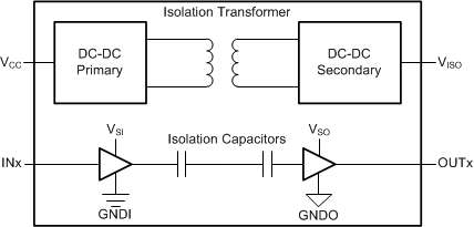
- VCC is the primary supply voltage referenced to GND1. VISO is the isolated supply voltage referenced to GND2.
- VSI and VSO can be either VCC or VISO depending on the channel direction
- VSI is the input-side supply voltage referenced to GNDI and VSO is the output-side supply voltage referenced to GNDO.