SWRS228B September 2019 – September 2024 IWR1843
PRODUCTION DATA
- 1
- 1 Features
- 2 Applications
- 3 Description
- 4 Functional Block Diagram
- 5 Device Comparison
- 6 Terminal Configuration and Functions
-
7 Specifications
- 7.1 Absolute Maximum Ratings
- 7.2 ESD Ratings
- 7.3 Power-On Hours (POH)
- 7.4 Recommended Operating Conditions
- 7.5 Power Supply Specifications
- 7.6 Power Consumption Summary
- 7.7 RF Specification
- 7.8 CPU Specifications
- 7.9 Thermal Resistance Characteristics for FCBGA Package [ABL0161]
- 7.10
Timing and Switching Characteristics
- 7.10.1 Power Supply Sequencing and Reset Timing
- 7.10.2 Input Clocks and Oscillators
- 7.10.3
Multibuffered / Standard Serial Peripheral Interface (MibSPI)
- 7.10.3.1 Peripheral Description
- 7.10.3.2
MibSPI Transmit and Receive RAM Organization
- 7.10.3.2.1 SPI Timing Conditions
- 7.10.3.2.2 SPI Controller Mode Switching Parameters (CLOCK PHASE = 0, SPICLK = output, SPISIMO = output, and SPISOMI = input) #GUID-C70CFB1F-161A-495B-85B8-62E1C643D037/T4362547-236 #GUID-C70CFB1F-161A-495B-85B8-62E1C643D037/T4362547-237 #GUID-C70CFB1F-161A-495B-85B8-62E1C643D037/T4362547-238
- 7.10.3.2.3 SPI Controller Mode Switching Parameters (CLOCK PHASE = 1, SPICLK = output, SPISIMO = output, and SPISOMI = input) #GUID-F724BCC6-8F26-42C4-8723-451EDE9A36D3/T4362547-244 #GUID-F724BCC6-8F26-42C4-8723-451EDE9A36D3/T4362547-245 #GUID-F724BCC6-8F26-42C4-8723-451EDE9A36D3/T4362547-246
- 7.10.3.3 SPI Peripheral Mode I/O Timings
- 7.10.3.4 Typical Interface Protocol Diagram (Peripheral Mode)
- 7.10.4 LVDS Interface Configuration
- 7.10.5 General-Purpose Input/Output
- 7.10.6 Controller Area Network Interface (DCAN)
- 7.10.7 Controller Area Network - Flexible Data-rate (CAN-FD)
- 7.10.8 Serial Communication Interface (SCI)
- 7.10.9 Inter-Integrated Circuit Interface (I2C)
- 7.10.10 Quad Serial Peripheral Interface (QSPI)
- 7.10.11 ETM Trace Interface
- 7.10.12 Data Modification Module (DMM)
- 7.10.13 JTAG Interface
- 8 Detailed Description
- 9 Monitoring and Diagnostics
- 10Applications, Implementation, and Layout
- 11Device and Documentation Support
- 12Revision History
- 13Mechanical, Packaging, and Orderable Information
Package Options
Mechanical Data (Package|Pins)
- ABL|161
Thermal pad, mechanical data (Package|Pins)
Orderable Information
8.4.1 ADC Channels (Service) for User Application
The IWR1843 device includes provision for an ADC service for user application, where the
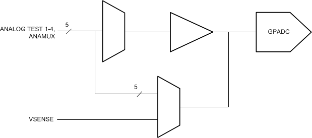
GPADC engine present inside the device can be used to measure up to six external voltages. The ADC1, ADC2, ADC3, ADC4, ADC5, and ADC6 pins are used for this purpose.
- ADC itself is controlled by TI firmware running inside the BIST subsystem and access to it for customer’s external voltage monitoring purpose is via ‘monitoring API’ calls routed to the BIST subsystem. This API could be linked with the user application running on MSS R4F.
- BIST subsystem firmware will internally schedule these measurements along with other RF and Analog monitoring operations. The API allows configuring the settling time (number of ADC samples to skip) and number of consecutive samples to take. At the end of a frame, the minimum, maximum and average of the readings will be reported for each of the monitored voltages.
GPADC Specifications:
- 625 Ksps SAR ADC
- 0 to 1.8V input range
- 10-bit resolution
- For 5 out of the 6 inputs, an optional internal buffer is available. Without the buffer, the ADC has a switched capacitor input load modeled with 5pF of sampling capacitance and 12pF parasitic capacitance (GPADC channel 6, the internal buffer is not available).

A. GPADC structures are
used for measuring the output of internal
temperature sensors. The accuracy of these
measurements is ±7°C.
Figure 8-6 ADC
Path