SWRS317 May   2023 IWR1843AOP

PRODUCTION DATA  

  1.   1
  2. Features
  3. Applications
  4. Description
    1. 3.1 Functional Block Diagram
  5. Revision History
  6. Device Comparison
    1. 5.1 Related Products
  7. Terminal Configuration and Functions
    1. 6.1 Pin Diagram
    2. 6.2 Pin Attributes
    3. 6.3 Signal Descriptions
      1. 6.3.1 Pin Functions - Digital and Analog [ALP Package]
  8. Specifications
    1. 7.1  Absolute Maximum Ratings
    2. 7.2  ESD Ratings
    3. 7.3  Power-On Hours (POH)
    4. 7.4  Recommended Operating Conditions
    5. 7.5  Power Supply Specifications
    6. 7.6  Power Consumption Summary
    7. 7.7  RF Specification
    8. 7.8  CPU Specifications
    9. 7.9  Thermal Resistance Characteristics for FCBGA Package [ALP0180A]
    10. 7.10 Timing and Switching Characteristics
      1. 7.10.1  Antenna Radiation Patterns
        1. 7.10.1.1 Antenna Radiation Patterns for Receiver
        2. 7.10.1.2 Antenna Radiation Patterns for Transmitter
      2. 7.10.2  Antenna Positions
      3. 7.10.3  Power Supply Sequencing and Reset Timing
      4. 7.10.4  Input Clocks and Oscillators
        1. 7.10.4.1 Clock Specifications
      5. 7.10.5  Multibuffered / Standard Serial Peripheral Interface (MibSPI)
        1. 7.10.5.1 Peripheral Description
        2. 7.10.5.2 MibSPI Transmit and Receive RAM Organization
          1. 7.10.5.2.1 SPI Timing Conditions
          2. 7.10.5.2.2 SPI Controller Mode Switching Parameters (CLOCK PHASE = 0, SPICLK = output, SPISIMO = output, and SPISOMI = input)
          3. 7.10.5.2.3 SPI Controller Mode Switching Parameters (CLOCK PHASE = 1, SPICLK = output, SPISIMO = output, and SPISOMI = input)
        3. 7.10.5.3 SPI Peripheral Mode I/O Timings
          1. 7.10.5.3.1 SPI Peripheral Mode Switching Parameters (SPICLK = input, SPISIMO = input, and SPISOMI = output)
        4. 7.10.5.4 Typical Interface Protocol Diagram (Peripheral Mode)
      6. 7.10.6  LVDS Interface Configuration
        1. 7.10.6.1 LVDS Interface Timings
      7. 7.10.7  General-Purpose Input/Output
        1. 7.10.7.1 Switching Characteristics for Output Timing versus Load Capacitance (CL) #GUID-A9917993-C388-4AAC-B9C6-6B2BF583E88E/T4362547-45 #GUID-A9917993-C388-4AAC-B9C6-6B2BF583E88E/T4362547-50
      8. 7.10.8  Controller Area Network Interface (DCAN)
        1. 7.10.8.1 Dynamic Characteristics for the DCANx TX and RX Pins
      9. 7.10.9  Controller Area Network - Flexible Data-rate (CAN-FD)
        1. 7.10.9.1 Dynamic Characteristics for the CANx TX and RX Pins
      10. 7.10.10 Serial Communication Interface (SCI)
        1. 7.10.10.1 SCI Timing Requirements
      11. 7.10.11 Inter-Integrated Circuit Interface (I2C)
        1. 7.10.11.1 I2C Timing Requirements #GUID-D26A1D00-D5E4-49AB-AFF7-B0ED1920A8A5/T4362547-185
      12. 7.10.12 Quad Serial Peripheral Interface (QSPI)
        1. 7.10.12.1 QSPI Timing Conditions
        2. 7.10.12.2 Timing Requirements for QSPI Input (Read) Timings #GUID-F4461E81-32E4-4CB7-B562-43AFC94843D1/T4362547-210 #GUID-F4461E81-32E4-4CB7-B562-43AFC94843D1/T4362547-209
        3. 7.10.12.3 QSPI Switching Characteristics
      13. 7.10.13 ETM Trace Interface
        1. 7.10.13.1 ETMTRACE Timing Conditions
        2. 7.10.13.2 ETM TRACE Switching Characteristics
      14. 7.10.14 Data Modification Module (DMM)
        1. 7.10.14.1 DMM Timing Requirements
      15. 7.10.15 JTAG Interface
        1. 7.10.15.1 JTAG Timing Conditions
        2. 7.10.15.2 Timing Requirements for IEEE 1149.1 JTAG
        3. 7.10.15.3 Switching Characteristics Over Recommended Operating Conditions for IEEE 1149.1 JTAG
  9. Detailed Description
    1. 8.1 Overview
    2. 8.2 Functional Block Diagram
    3. 8.3 Subsystems
      1. 8.3.1 RF and Analog Subsystem
        1. 8.3.1.1 Clock Subsystem
        2. 8.3.1.2 Transmit Subsystem
        3. 8.3.1.3 Receive Subsystem
      2. 8.3.2 Processor Subsystem
      3. 8.3.3 Host Interface
      4. 8.3.4 Main Subsystem Cortex-R4F Memory Map
      5. 8.3.5 DSP Subsystem Memory Map
    4. 8.4 Other Subsystems
      1. 8.4.1 ADC Channels (Service) for User Application
        1. 8.4.1.1 GP-ADC Parameter
  10. Monitoring and Diagnostics
    1. 9.1 Monitoring and Diagnostic Mechanisms
      1. 9.1.1 Error Signaling Module
  11. 10Applications, Implementation, and Layout
    1. 10.1 Application Information
    2. 10.2 Reference Schematic
  12. 11Device and Documentation Support
    1. 11.1 Device Nomenclature
    2. 11.2 Tools and Software
    3. 11.3 Documentation Support
    4. 11.4 Support Resources
    5. 11.5 Trademarks
    6. 11.6 Electrostatic Discharge Caution
    7. 11.7 Glossary
  13. 12Mechanical, Packaging, and Orderable Information
    1. 12.1 Packaging Information

Package Options

Mechanical Data (Package|Pins)
Thermal pad, mechanical data (Package|Pins)
Orderable Information

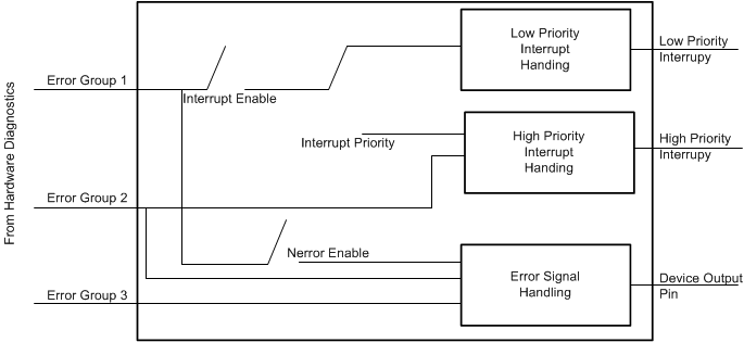
Error Signaling Module

When a diagnostic detects a fault, the error must be indicated. IWR1843AOP architecture provides aggregation of fault indication from internal diagnostic mechanisms using a peripheral logic known as the error signaling module (ESM). The ESM provides mechanisms to classify faults by severity and allows programmable error response. Below is the high level block diagram for ESM module.
GUID-26CF0444-C19D-48EC-88EB-57BC2EB67DC0-low.gifFigure 9-1 ESM Module Diagram