SWRS313A July 2023 – June 2024 IWRL1432
PRODUCTION DATA
- 1
- 1 Features
- 2 Applications
- 3 Description
- 4 Functional Block Diagram
- 5 Device Comparison
- 6 Terminal Configurations and Functions
-
7 Specifications
- 7.1 Absolute Maximum Ratings
- 7.2 ESD Ratings
- 7.3 Power-On Hours (POH)
- 7.4 Recommended Operating Conditions
- 7.5 VPP Specifications for One-Time Programmable (OTP) eFuses
- 7.6
Power Supply Specifications
- 7.6.1 Power Optimized 3.3V I/O Topology
- 7.6.2 BOM Optimized 3.3V I/O Topology
- 7.6.3 Power Optimized 1.8V I/O Topology
- 7.6.4 BOM Optimized 1.8V I/O Topology
- 7.6.5 System Topologies
- 7.6.6 Internal LDO output decoupling capacitor and layout conditions for BOM optimized topology
- 7.6.7 Noise and Ripple Specifications
- 7.7 Power Save Modes
- 7.8 Peak Current Requirement per Voltage Rail
- 7.9 RF Specification
- 7.10 Supported Front End features
- 7.11 CPU Specifications
- 7.12 Thermal Resistance Characteristics
- 7.13
Timing and Switching Characteristics
- 7.13.1 Power Supply Sequencing and Reset Timing
- 7.13.2 Synchronized Frame Triggering
- 7.13.3 Input Clocks and Oscillators
- 7.13.4 MultiChannel buffered / Standard Serial Peripheral Interface (McSPI)
- 7.13.5 RDIF Interface Configuration
- 7.13.6 General-Purpose Input/Output
- 7.13.7 Controller Area Network - Flexible Data-rate (CAN-FD)
- 7.13.8 Serial Communication Interface (SCI)
- 7.13.9 Inter-Integrated Circuit Interface (I2C)
- 7.13.10 Quad Serial Peripheral Interface (QSPI)
- 7.13.11 JTAG Interface
- 8 Detailed Description
- 9 Monitoring and Diagnostics
- 10Applications, Implementation, and Layout
- 11Device and Documentation Support
- 12Revision History
- 13Mechanical, Packaging, and Orderable Information
Package Options
Mechanical Data (Package|Pins)
- AMF|102
Thermal pad, mechanical data (Package|Pins)
Orderable Information
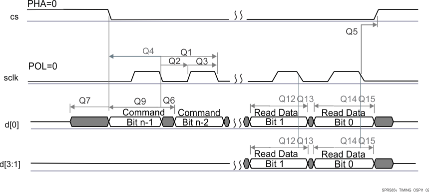
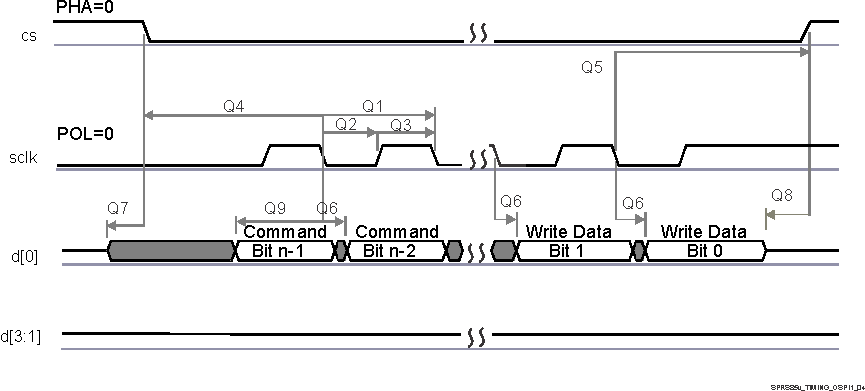
7.13.10.3 QSPI Switching Characteristics
| NO. | PARAMETER | MIN | TYP | MAX | UNIT | |
|---|---|---|---|---|---|---|
| Q1 | tc(SCLK) | Cycle time, sclk | 12.5 | ns | ||
| Q2 | tw(SCLKL) | Pulse duration, sclk low | Y*P – 3(1)(2) | ns | ||
| Q3 | tw(SCLKH) | Pulse duration, sclk high | Y*P – 3(1)(2) | ns | ||
| Q4 | td(CS-SCLK) | Delay time, sclk falling edge to cs active edge | –M*P – 1(2)(3) | –M*P + 2.5(2)(3) | ns | |
| Q5 | td(SCLK-CS) | Delay time, sclk falling edge to cs inactive edge | N*P – 1(2)(3) | N*P + 2.5(2)(3) | ns | |
| Q6 | td(SCLK-D1) | Delay time, sclk falling edge to d[1] transition | –2 | 4 | ns | |
| Q7 | tena(CS-D1LZ) | Enable time, cs active edge to d[1] driven (lo-z) | –P – 4(2) | –P +1(2) | ns | |
| Q8 | tdis(CS-D1Z) | Disable time, cs active edge to d[1] tri-stated (hi-z) | –P – 4(2) | –P +1(2) | ns | |
| Q9 | td(SCLK-D1) | Delay time, sclk first falling edge to first d[1] transition (for PHA = 0 only) | –2 – P(2) | 4– P(2) | ns | |
| Q12 | tsu(D-SCLK) | Setup time, d[3:0] valid before falling sclk edge | 5 | ns | ||
| Q13 | th(SCLK-D) | Hold time, d[3:0] valid after falling sclk edge | 1 | ns | ||
| Q14 | tsu(D-SCLK) | Setup time, final d[3:0] bit valid before final falling sclk edge | 5 — P(2) | ns | ||
| Q15 | th(SCLK-D) | Hold time, final d[3:0] bit valid after final falling sclk edge | 1 + P(2) | ns | ||
(1) The Y parameter is defined as follows: If DCLK_DIV is 0 or ODD then, Y equals 0.5. If DCLK_DIV is EVEN then, Y equals (DCLK_DIV/2) / (DCLK_DIV+1). For best performance, it is recommended to use a DCLK_DIV of 0 or ODD to minimize the duty cycle distortion. All required details about clock division factor DCLK_DIV can be found in the device-specific Technical Reference Manual.
(2) P = SCLK period in ns.
(3) M = QSPI_SPI_DC_REG.DDx + 1, N = 2
 Figure 7-18 QSPI Read (Clock Mode 0)
 Figure 7-19 QSPI Write (Clock Mode 0)