SWRS313A July   2023  – June 2024 IWRL1432

PRODUCTION DATA  

  1.   1
  2. Features
  3. Applications
  4. Description
  5. Functional Block Diagram
  6. Device Comparison
    1. 5.1 Related Products
  7. Terminal Configurations and Functions
    1. 6.1 Pin Diagrams
    2. 6.2 Signal Descriptions
      1.      11
      2.      12
      3.      13
      4.      14
      5.      15
      6.      16
      7.      17
      8.      18
      9.      19
      10.      20
      11.      21
      12.      22
      13.      23
      14.      24
      15.      25
      16.      26
    3.     27
  8. Specifications
    1. 7.1  Absolute Maximum Ratings
    2. 7.2  ESD Ratings
    3. 7.3  Power-On Hours (POH)
    4. 7.4  Recommended Operating Conditions
    5. 7.5  VPP Specifications for One-Time Programmable (OTP) eFuses
      1. 7.5.1 Recommended Operating Conditions for OTP eFuse Programming
      2. 7.5.2 Hardware Requirements
      3. 7.5.3 Impact to Your Hardware Warranty
    6. 7.6  Power Supply Specifications
      1. 7.6.1 Power Optimized 3.3V I/O Topology
      2. 7.6.2 BOM Optimized 3.3V I/O Topology
      3. 7.6.3 Power Optimized 1.8V I/O Topology
      4. 7.6.4 BOM Optimized 1.8V I/O Topology
      5. 7.6.5 System Topologies
        1. 7.6.5.1 Power Topologies
          1. 7.6.5.1.1 BOM Optimized Mode
          2. 7.6.5.1.2 Power Optimized Mode
      6. 7.6.6 Internal LDO output decoupling capacitor and layout conditions for BOM optimized topology
        1. 7.6.6.1 Single-capacitor rail
          1. 7.6.6.1.1 1.2V Digital LDO
        2. 7.6.6.2 Two-capacitor rail
          1. 7.6.6.2.1 1.2V RF LDO
          2. 7.6.6.2.2 1.2V SRAM LDO
          3. 7.6.6.2.3 1.0V RF LDO
      7. 7.6.7 Noise and Ripple Specifications
    7. 7.7  Power Save Modes
      1. 7.7.1 Typical Power Consumption Numbers
    8. 7.8  Peak Current Requirement per Voltage Rail
    9. 7.9  RF Specification
    10. 7.10 Supported Front End features
    11. 7.11 CPU Specifications
    12. 7.12 Thermal Resistance Characteristics
    13. 7.13 Timing and Switching Characteristics
      1. 7.13.1  Power Supply Sequencing and Reset Timing
      2. 7.13.2  Synchronized Frame Triggering
      3. 7.13.3  Input Clocks and Oscillators
        1. 7.13.3.1 Clock Specifications
      4. 7.13.4  MultiChannel buffered / Standard Serial Peripheral Interface (McSPI)
        1. 7.13.4.1 McSPI Features
        2. 7.13.4.2 SPI Timing Conditions
        3. 7.13.4.3 SPI—Controller Mode
          1. 7.13.4.3.1 Timing and Switching Requirements for SPI - Controller Mode
          2. 7.13.4.3.2 Timing and Switching Characteristics for SPI Output Timings—Controller Mode
        4. 7.13.4.4 SPI—Peripheral Mode
          1. 7.13.4.4.1 Timing and Switching Requirements for SPI - Peripheral Mode
          2. 7.13.4.4.2 Timing and Switching Characteristics for SPI Output Timings—Secondary Mode
      5. 7.13.5  RDIF Interface Configuration
        1. 7.13.5.1 RDIF Interface Timings
        2. 7.13.5.2 RDIF Data Format
      6. 7.13.6  General-Purpose Input/Output
        1. 7.13.6.1 Switching Characteristics for Output Timing versus Load Capacitance (CL)
      7. 7.13.7  Controller Area Network - Flexible Data-rate (CAN-FD)
        1. 7.13.7.1 Dynamic Characteristics for the CANx TX and RX Pins
      8. 7.13.8  Serial Communication Interface (SCI)
        1. 7.13.8.1 SCI Timing Requirements
      9. 7.13.9  Inter-Integrated Circuit Interface (I2C)
        1. 7.13.9.1 I2C Timing Requirements
      10. 7.13.10 Quad Serial Peripheral Interface (QSPI)
        1. 7.13.10.1 QSPI Timing Conditions
        2. 7.13.10.2 Timing Requirements for QSPI Input (Read) Timings
        3. 7.13.10.3 QSPI Switching Characteristics
      11. 7.13.11 JTAG Interface
        1. 7.13.11.1 JTAG Timing Conditions
        2. 7.13.11.2 Timing Requirements for IEEE 1149.1 JTAG
        3. 7.13.11.3 Switching Characteristics Over Recommended Operating Conditions for IEEE 1149.1 JTAG
  9. Detailed Description
    1. 8.1 Overview
    2. 8.2 Functional Block Diagram
    3. 8.3 Subsystems
      1. 8.3.1 RF and Analog Subsystem
      2. 8.3.2 Clock Subsystem
      3. 8.3.3 Transmit Subsystem
      4. 8.3.4 Receive Subsystem
      5. 8.3.5 Processor Subsystem
      6. 8.3.6 Host Interface
      7. 8.3.7 Application Subsystem
      8. 8.3.8 Hardware Accelerator (HWA1.2) Features
        1. 8.3.8.1 Hardware Accelerator Feature Differences Between HWA1.1 and HWA1.2
    4. 8.4 Other Subsystems
      1. 8.4.1 GPADC Channels (Service) for User Application
      2. 8.4.2 GPADC Parameters
    5. 8.5 Memory Partitioning Options
    6. 8.6 Boot Modes
  10. Monitoring and Diagnostics
  11. 10Applications, Implementation, and Layout
    1. 10.1 Application Information
    2. 10.2 Reference Schematic
  12. 11Device and Documentation Support
    1. 11.1 Device Nomenclature
    2. 11.2 Tools and Software
    3. 11.3 Documentation Support
    4. 11.4 Support Resources
    5. 11.5 Trademarks
    6. 11.6 Electrostatic Discharge Caution
    7. 11.7 Glossary
  13. 12Revision History
  14. 13Mechanical, Packaging, and Orderable Information

Package Options

Mechanical Data (Package|Pins)
  • AMF|102
Thermal pad, mechanical data (Package|Pins)
Orderable Information

Processor Subsystem

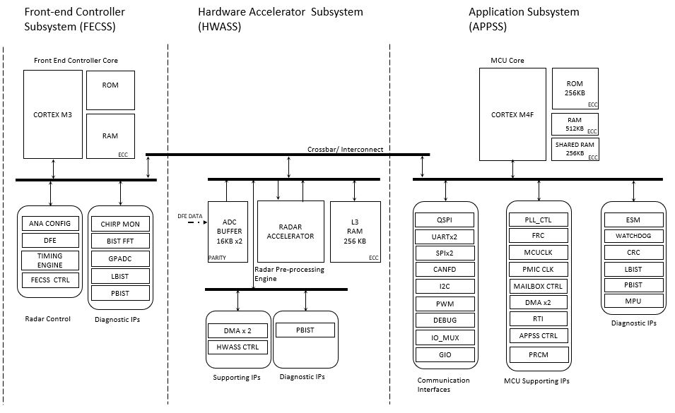
IWRL1432 Processor Subsystem Figure 8-5 Processor Subsystem

Figure 8-5 shows the block diagram for customer programmable processor subsystems in the IWRL1432 device. At a high level there are two customer programmable subsystems, as shown separated by a dotted line in the diagram. The left hand side shows the HWA, a high-bandwidth interconnect for high performance (64-bit, 80MHz), and associated peripherals data transfer. RDIF interface for Measurement data output, L3 Radar data cube memory, the ADC buffers, the CRC engine, and data handshake memory (additional memory provided on interconnect).

The right side of the diagram shows the Main Subsystem. The Main Subsystem is the brain of the device and controls all the device peripherals and house-keeping activities of the device. The Main Subsystem contains Cortex-M4F processor and associated peripherals and house-keeping components such as DMAs, CRC and Peripherals (I2C, UART, SPIs, CAN, PMIC clocking module, PWM, and others) connected to Main Interconnect through Peripheral Central Resource (PCR interconnect).