SWRS313A July 2023 – June 2024 IWRL1432
PRODUCTION DATA
- 1
- 1 Features
- 2 Applications
- 3 Description
- 4 Functional Block Diagram
- 5 Device Comparison
- 6 Terminal Configurations and Functions
-
7 Specifications
- 7.1 Absolute Maximum Ratings
- 7.2 ESD Ratings
- 7.3 Power-On Hours (POH)
- 7.4 Recommended Operating Conditions
- 7.5 VPP Specifications for One-Time Programmable (OTP) eFuses
- 7.6
Power Supply Specifications
- 7.6.1 Power Optimized 3.3V I/O Topology
- 7.6.2 BOM Optimized 3.3V I/O Topology
- 7.6.3 Power Optimized 1.8V I/O Topology
- 7.6.4 BOM Optimized 1.8V I/O Topology
- 7.6.5 System Topologies
- 7.6.6 Internal LDO output decoupling capacitor and layout conditions for BOM optimized topology
- 7.6.7 Noise and Ripple Specifications
- 7.7 Power Save Modes
- 7.8 Peak Current Requirement per Voltage Rail
- 7.9 RF Specification
- 7.10 Supported Front End features
- 7.11 CPU Specifications
- 7.12 Thermal Resistance Characteristics
- 7.13
Timing and Switching Characteristics
- 7.13.1 Power Supply Sequencing and Reset Timing
- 7.13.2 Synchronized Frame Triggering
- 7.13.3 Input Clocks and Oscillators
- 7.13.4 MultiChannel buffered / Standard Serial Peripheral Interface (McSPI)
- 7.13.5 RDIF Interface Configuration
- 7.13.6 General-Purpose Input/Output
- 7.13.7 Controller Area Network - Flexible Data-rate (CAN-FD)
- 7.13.8 Serial Communication Interface (SCI)
- 7.13.9 Inter-Integrated Circuit Interface (I2C)
- 7.13.10 Quad Serial Peripheral Interface (QSPI)
- 7.13.11 JTAG Interface
- 8 Detailed Description
- 9 Monitoring and Diagnostics
- 10Applications, Implementation, and Layout
- 11Device and Documentation Support
- 12Revision History
- 13Mechanical, Packaging, and Orderable Information
Package Options
Mechanical Data (Package|Pins)
- AMF|102
Thermal pad, mechanical data (Package|Pins)
Orderable Information
7.9 RF Specification
Over recommended operating conditions (unless otherwise
noted)
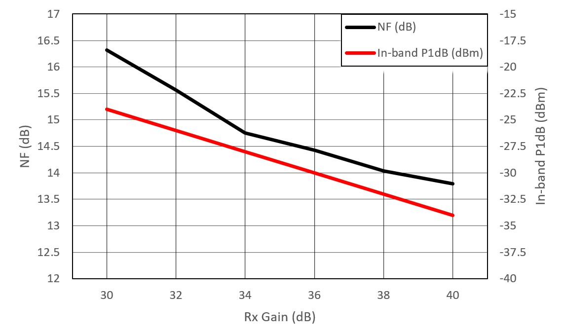
 Figure 7-6 Noise Figure, In-band P1dB vs
Receiver Gain
| PARAMETER | MIN | TYP | MAX | UNIT | ||
|---|---|---|---|---|---|---|
| Receiver(1) | Noise figure | 76 to 81 GHz | 14 | dB | ||
| 1-dB compression point (Out Of Band)(2) | –10 | dBm | ||||
| Maximum gain | 40 | dB | ||||
| Gain range | 10 | dB | ||||
| Gain step size | 2 | dB | ||||
| IF bandwidth(3) | 5 | MHz | ||||
| ADC sampling rate (real) | 12.5 | Msps | ||||
| ADC resolution | 12 | Bits | ||||
| S11 | -10 | dB | ||||
| Transmitter(1) | Output Power | 11 | dBm | |||
| S11 | -10 | dB | ||||
| Clock subsystem | Frequency range | 76 | 81 | GHz | ||
| Ramp rate |
400 |
MHz/µs | ||||
| Phase noise at 1-MHz offset | 76 to 81 GHz | –89 | dBc/Hz | |||
(1) The polarity of LO signal for TX2
is inverted with respect to TX1, hence the phase of the signal is expected to
have 1800 offset. Enabling BPM on a transmitter chain will create
additional 1800 phase offset on that chain. The polarity of LO signal
for RX2 is inverted with respect to RX1 and RX3, hence the phase of the signal
is expected to have 1800 offset. This can be taken care during
post-processing, in HWA or external processing.
(2) 1-dB Compression Point (Out Of Band) is measured by feed a
Continuous wave Tone well below the HPF cut-off frequency.
(3) The analog IF stages include high-pass filtering, with configurable
first-order high-pass corner frequency. The set of available HPF corners is
summarized as follows:
The filtering performed by the digital baseband chain is targeted to
provide less than ±0.5 dB pass-band ripple/droop.
| Available HPF Corner Frequencies (kHz) |
| 175, 350, 700, 1400 |
Figure 7-6 shows variations of noise figure and in-band P1dB parameters with respect to receiver gain programmed.
 Figure 7-6 Noise Figure, In-band P1dB vs
Receiver Gain