SWRS323 November   2023  – April 2024 IWRL6432AOP

ADVANCE INFORMATION  

  1.   1
  2. Features
  3. Applications
  4. Description
  5. Functional Block Diagram
  6. Device Comparison
    1. 5.1 Related Products
  7. Terminal Configurations and Functions
    1. 6.1 Pin Diagrams
    2.     10
    3. 6.2 Signal Descriptions
      1.      12
      2.      13
      3.      14
      4.      15
      5.      16
      6.      17
      7.      18
      8.      19
      9.      20
      10.      21
      11.      22
      12.      23
      13.      24
      14.      25
      15.      26
      16.      27
  8. Specifications
    1. 7.1  Absolute Maximum Ratings
    2. 7.2  ESD Ratings
    3. 7.3  Power-On Hours (POH)
    4. 7.4  Recommended Operating Conditions
    5. 7.5  VPP Specifications for One-Time Programmable (OTP) eFuses
      1. 7.5.1 Recommended Operating Conditions for OTP eFuse Programming
      2. 7.5.2 Hardware Requirements
      3. 7.5.3 Impact to Your Hardware Warranty
    6. 7.6  Power Supply Specifications
      1. 7.6.1 Power Optimized 3.3V I/O Topology
      2. 7.6.2 Power Optimized 1.8V I/O Topology
      3. 7.6.3 BOM Optimized 3.3V I/O Topology
      4. 7.6.4 BOM Optimized 1.8V I/O Topology
      5. 7.6.5 System Topologies
        1. 7.6.5.1 Power Topologies
          1. 7.6.5.1.1 BOM Optimized Mode
          2. 7.6.5.1.2 Power Optimized Mode
      6. 7.6.6 Internal LDO output decoupling capacitor and layout conditions for BOM optimized topology
        1. 7.6.6.1 Single-capacitor rail
          1. 7.6.6.1.1 1.2V Digital LDO
        2. 7.6.6.2 Two-capacitor rail
          1. 7.6.6.2.1 1.2V RF LDO
          2. 7.6.6.2.2 1.2V SRAM LDO
          3. 7.6.6.2.3 1.0V RF LDO
      7. 7.6.7 Noise and Ripple Specifications
    7. 7.7  Power Save Modes
      1. 7.7.1 Typical Power Consumption Numbers
    8. 7.8  Peak Current Requirement per Voltage Rail
    9. 7.9  Supported DFE Features
    10. 7.10 RF Specification
    11. 7.11 CPU Specifications
    12. 7.12 Thermal Resistance Characteristics
    13. 7.13 Antenna Radiation Patterns
      1. 7.13.1 Antenna Radiation Patterns for Receiver
      2. 7.13.2 Antenna Radiation Patterns for Transmitter
    14. 7.14 Antenna Positions
    15. 7.15 Timing and Switching Characteristics
      1. 7.15.1  Power Supply Sequencing and Reset Timing
      2. 7.15.2  Synchronized Frame Triggering
      3. 7.15.3  Input Clocks and Oscillators
        1. 7.15.3.1 Clock Specifications
      4. 7.15.4  MultiChannel buffered / Standard Serial Peripheral Interface (McSPI)
        1. 7.15.4.1 McSPI Features
        2. 7.15.4.2 SPI Timing Conditions
        3. 7.15.4.3 SPI—Controller Mode
          1. 7.15.4.3.1 Timing and Switching Requirements for SPI - Controller Mode
          2. 7.15.4.3.2 Timing and Switching Characteristics for SPI Output Timings—Controller Mode
        4. 7.15.4.4 SPI—Peripheral Mode
          1. 7.15.4.4.1 Timing and Switching Requirements for SPI - Peripheral Mode
          2. 7.15.4.4.2 Timing and Switching Characteristics for SPI Output Timings—Secondary Mode
      5. 7.15.5  RDIF Interface Configuration
        1. 7.15.5.1 RDIF Interface Timings
        2. 7.15.5.2 RDIF Data Format
      6. 7.15.6  General-Purpose Input/Output
        1. 7.15.6.1 Switching Characteristics for Output Timing versus Load Capacitance (CL)
      7. 7.15.7  Controller Area Network - Flexible Data-rate (CAN-FD)
        1. 7.15.7.1 Dynamic Characteristics for the CANx TX and RX Pins
      8. 7.15.8  Serial Communication Interface (SCI)
        1. 7.15.8.1 SCI Timing Requirements
      9. 7.15.9  Inter-Integrated Circuit Interface (I2C)
        1. 7.15.9.1 I2C Timing Requirements
      10. 7.15.10 Quad Serial Peripheral Interface (QSPI)
        1. 7.15.10.1 QSPI Timing Conditions
        2. 7.15.10.2 Timing Requirements for QSPI Input (Read) Timings
        3. 7.15.10.3 QSPI Switching Characteristics
      11. 7.15.11 JTAG Interface
        1. 7.15.11.1 JTAG Timing Conditions
        2. 7.15.11.2 Timing Requirements for IEEE 1149.1 JTAG
        3. 7.15.11.3 Switching Characteristics Over Recommended Operating Conditions for IEEE 1149.1 JTAG
  9. Detailed Description
    1. 8.1 Overview
    2. 8.2 Functional Block Diagram
    3. 8.3 Subsystems
      1. 8.3.1 RF and Analog Subsystem
      2. 8.3.2 Clock Subsystem
      3. 8.3.3 Transmit Subsystem
      4. 8.3.4 Receive Subsystem
      5. 8.3.5 Processor Subsystem
      6. 8.3.6 Host Interface
      7. 8.3.7 Application Subsystem Cortex-M4F
      8. 8.3.8 Hardware Accelerator (HWA1.2) Features
        1. 8.3.8.1 Hardware Accelerator Feature Differences Between HWA1.1 and HWA1.2
    4. 8.4 Other Subsystems
      1. 8.4.1 GPADC Channels (Service) for User Application
      2. 8.4.2 GPADC Parameters
    5. 8.5 Memory Partitioning Options
    6. 8.6 Boot Modes
  10. Monitoring and Diagnostics
  11. 10Applications, Implementation, and Layout
    1. 10.1 Application Information
    2. 10.2 Reference Schematic
  12. 11Device and Documentation Support
    1. 11.1 Device Nomenclature
    2. 11.2 Tools and Software
    3. 11.3 Documentation Support
    4. 11.4 Support Resources
    5. 11.5 Trademarks
    6. 11.6 Electrostatic Discharge Caution
    7. 11.7 Glossary
  13. 12Revision History
  14. 13Mechanical, Packaging, and Orderable Information

Package Options

Mechanical Data (Package|Pins)
  • AMY|101
Thermal pad, mechanical data (Package|Pins)
Orderable Information

GPADC Channels (Service) for User Application

The IWRL6432AOP device includes provision for an ADC service for user application, where the GPADC engine present inside the device can be used to measure up to two external voltages. The GPADC1 is used for this purpose.

  • GPADC itself is controlled by TI firmware running inside the FEC sub-system and access to it for customer’s external voltage monitoring purpose is via ‘APPSS’ calls routed to the FEC subsystem. This API could be linked with the user application running on APPSS Cortex M4F®.
  • Device Firmware package (DFP) provides APIs to configure and measure these signals. The API allows configuring the settling time (number of ADC samples to skip) and number of consecutive samples to take. At the end of a frame, the minimum, maximum and average of the readings will be reported for each of the monitored voltages.
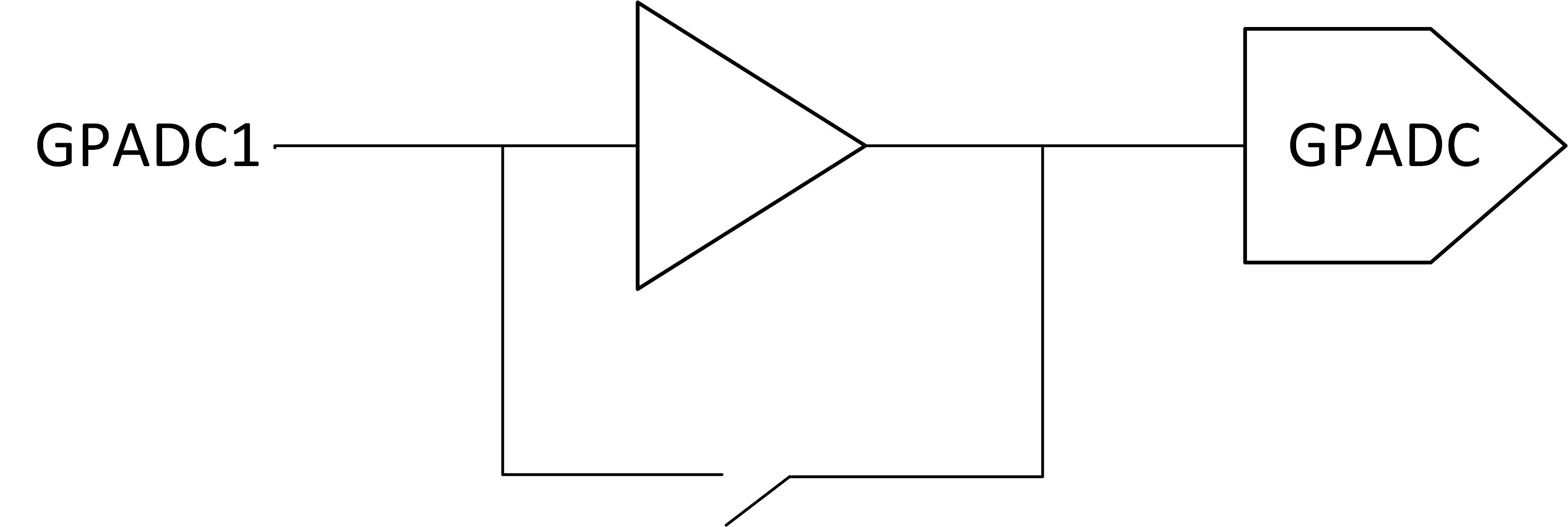
GUID-729FEBB2-47D9-4459-B230-5E0DC13BF716-low.png Figure 8-6 GPADC Path

GPADC structures are used for measuring the output of internal temperature sensors. The accuracy of these measurements is ±7°C.