SWRS323 November   2023  – April 2024 IWRL6432AOP

ADVANCE INFORMATION  

  1.   1
  2. Features
  3. Applications
  4. Description
  5. Functional Block Diagram
  6. Device Comparison
    1. 5.1 Related Products
  7. Terminal Configurations and Functions
    1. 6.1 Pin Diagrams
    2.     10
    3. 6.2 Signal Descriptions
      1.      12
      2.      13
      3.      14
      4.      15
      5.      16
      6.      17
      7.      18
      8.      19
      9.      20
      10.      21
      11.      22
      12.      23
      13.      24
      14.      25
      15.      26
      16.      27
  8. Specifications
    1. 7.1  Absolute Maximum Ratings
    2. 7.2  ESD Ratings
    3. 7.3  Power-On Hours (POH)
    4. 7.4  Recommended Operating Conditions
    5. 7.5  VPP Specifications for One-Time Programmable (OTP) eFuses
      1. 7.5.1 Recommended Operating Conditions for OTP eFuse Programming
      2. 7.5.2 Hardware Requirements
      3. 7.5.3 Impact to Your Hardware Warranty
    6. 7.6  Power Supply Specifications
      1. 7.6.1 Power Optimized 3.3V I/O Topology
      2. 7.6.2 Power Optimized 1.8V I/O Topology
      3. 7.6.3 BOM Optimized 3.3V I/O Topology
      4. 7.6.4 BOM Optimized 1.8V I/O Topology
      5. 7.6.5 System Topologies
        1. 7.6.5.1 Power Topologies
          1. 7.6.5.1.1 BOM Optimized Mode
          2. 7.6.5.1.2 Power Optimized Mode
      6. 7.6.6 Internal LDO output decoupling capacitor and layout conditions for BOM optimized topology
        1. 7.6.6.1 Single-capacitor rail
          1. 7.6.6.1.1 1.2V Digital LDO
        2. 7.6.6.2 Two-capacitor rail
          1. 7.6.6.2.1 1.2V RF LDO
          2. 7.6.6.2.2 1.2V SRAM LDO
          3. 7.6.6.2.3 1.0V RF LDO
      7. 7.6.7 Noise and Ripple Specifications
    7. 7.7  Power Save Modes
      1. 7.7.1 Typical Power Consumption Numbers
    8. 7.8  Peak Current Requirement per Voltage Rail
    9. 7.9  Supported DFE Features
    10. 7.10 RF Specification
    11. 7.11 CPU Specifications
    12. 7.12 Thermal Resistance Characteristics
    13. 7.13 Antenna Radiation Patterns
      1. 7.13.1 Antenna Radiation Patterns for Receiver
      2. 7.13.2 Antenna Radiation Patterns for Transmitter
    14. 7.14 Antenna Positions
    15. 7.15 Timing and Switching Characteristics
      1. 7.15.1  Power Supply Sequencing and Reset Timing
      2. 7.15.2  Synchronized Frame Triggering
      3. 7.15.3  Input Clocks and Oscillators
        1. 7.15.3.1 Clock Specifications
      4. 7.15.4  MultiChannel buffered / Standard Serial Peripheral Interface (McSPI)
        1. 7.15.4.1 McSPI Features
        2. 7.15.4.2 SPI Timing Conditions
        3. 7.15.4.3 SPI—Controller Mode
          1. 7.15.4.3.1 Timing and Switching Requirements for SPI - Controller Mode
          2. 7.15.4.3.2 Timing and Switching Characteristics for SPI Output Timings—Controller Mode
        4. 7.15.4.4 SPI—Peripheral Mode
          1. 7.15.4.4.1 Timing and Switching Requirements for SPI - Peripheral Mode
          2. 7.15.4.4.2 Timing and Switching Characteristics for SPI Output Timings—Secondary Mode
      5. 7.15.5  RDIF Interface Configuration
        1. 7.15.5.1 RDIF Interface Timings
        2. 7.15.5.2 RDIF Data Format
      6. 7.15.6  General-Purpose Input/Output
        1. 7.15.6.1 Switching Characteristics for Output Timing versus Load Capacitance (CL)
      7. 7.15.7  Controller Area Network - Flexible Data-rate (CAN-FD)
        1. 7.15.7.1 Dynamic Characteristics for the CANx TX and RX Pins
      8. 7.15.8  Serial Communication Interface (SCI)
        1. 7.15.8.1 SCI Timing Requirements
      9. 7.15.9  Inter-Integrated Circuit Interface (I2C)
        1. 7.15.9.1 I2C Timing Requirements
      10. 7.15.10 Quad Serial Peripheral Interface (QSPI)
        1. 7.15.10.1 QSPI Timing Conditions
        2. 7.15.10.2 Timing Requirements for QSPI Input (Read) Timings
        3. 7.15.10.3 QSPI Switching Characteristics
      11. 7.15.11 JTAG Interface
        1. 7.15.11.1 JTAG Timing Conditions
        2. 7.15.11.2 Timing Requirements for IEEE 1149.1 JTAG
        3. 7.15.11.3 Switching Characteristics Over Recommended Operating Conditions for IEEE 1149.1 JTAG
  9. Detailed Description
    1. 8.1 Overview
    2. 8.2 Functional Block Diagram
    3. 8.3 Subsystems
      1. 8.3.1 RF and Analog Subsystem
      2. 8.3.2 Clock Subsystem
      3. 8.3.3 Transmit Subsystem
      4. 8.3.4 Receive Subsystem
      5. 8.3.5 Processor Subsystem
      6. 8.3.6 Host Interface
      7. 8.3.7 Application Subsystem Cortex-M4F
      8. 8.3.8 Hardware Accelerator (HWA1.2) Features
        1. 8.3.8.1 Hardware Accelerator Feature Differences Between HWA1.1 and HWA1.2
    4. 8.4 Other Subsystems
      1. 8.4.1 GPADC Channels (Service) for User Application
      2. 8.4.2 GPADC Parameters
    5. 8.5 Memory Partitioning Options
    6. 8.6 Boot Modes
  10. Monitoring and Diagnostics
  11. 10Applications, Implementation, and Layout
    1. 10.1 Application Information
    2. 10.2 Reference Schematic
  12. 11Device and Documentation Support
    1. 11.1 Device Nomenclature
    2. 11.2 Tools and Software
    3. 11.3 Documentation Support
    4. 11.4 Support Resources
    5. 11.5 Trademarks
    6. 11.6 Electrostatic Discharge Caution
    7. 11.7 Glossary
  13. 12Revision History
  14. 13Mechanical, Packaging, and Orderable Information

Package Options

Mechanical Data (Package|Pins)
  • AMY|101
Thermal pad, mechanical data (Package|Pins)
Orderable Information

Supported DFE Features

  • TX output back-off
    • From 0dB to 26dB TX back-off in steps of 1dB is supported

  • RX gain
    • Real RX channels
    • Total RX gain range of 30 dB to 40dB, in 2dB steps
  • VCO
    • Single VCO covering entire RF sweep bandwidth up to 7GHz.
  • High-pass filter
    • Supports corner frequency options 175kHz, 350kHz, 700kHz, 1400kHz
    • First-order high pass filter only
  • Low-pass filter
    • Max IF bandwidth supported is 5MHz
    • 40dB stopband rejection, two filtering options supported
    • 90% visibility – IF bandwidth is 90% of Nyquist (has longer setting time due to larger filter length)
    • 80% visibility – IF bandwidth is 80% of Nyquist and is 30% faster due to quicker settling time, compared with 90% visibility
  • Supported ADC sampling rates
    • 1.0, 1.25, 1.667, 2.0, 2.5, 4.0, 5.0, 6.667, 7.692, 10.0, 12.5Msps
  • Timing Engine
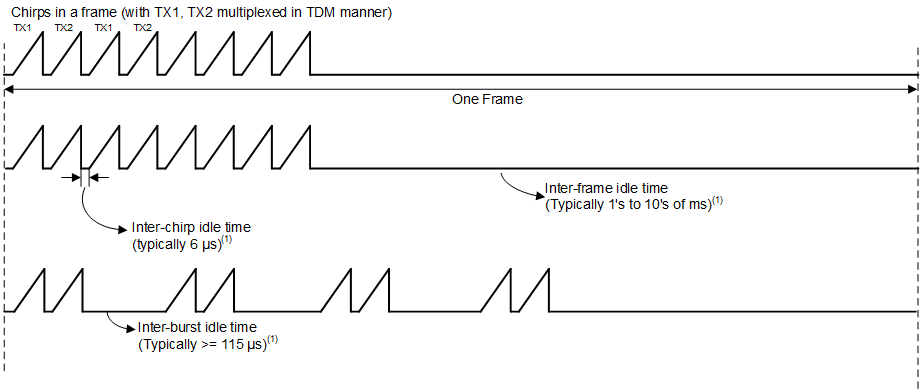
    • Support for chirps, bursts and frames
      • Longer frame idle time gives more power saving than a longer burst idle time. Further, a longer chirp idle time gives lesser power saving than a longer burst idle time. For more details please refer power calculator in the mmWave sensing estimator.
      • Chirp accumulation (averaging) possible across closely spaced chirps to reduce memory requirement
    • Provision for per-chirp dithering of parameters
GUID-14EFC0F2-F89C-4A16-87A3-E51BB50CB5C8-low.png
  1. Refer to DFP API documentation
Figure 7-6 Chip Profile Supported by Timing Engine