SLPS730B august 2021 – august 2023 JFE2140
PRODUCTION DATA
- 1
- 1 Features
- 2 Applications
- 3 Description
- 4 Revision History
- 5 Pin Configuration and Functions
- 6 Specifications
- 7 Parameter Measurement Information
- 8 Detailed Description
- 9 Application and Implementation
- 10Device and Documentation Support
- 11Mechanical, Packaging, and Orderable Information
Package Options
Mechanical Data (Package|Pins)
Thermal pad, mechanical data (Package|Pins)
- DSG|8
Orderable Information
3 Description
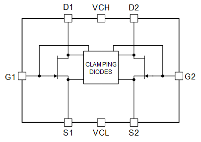
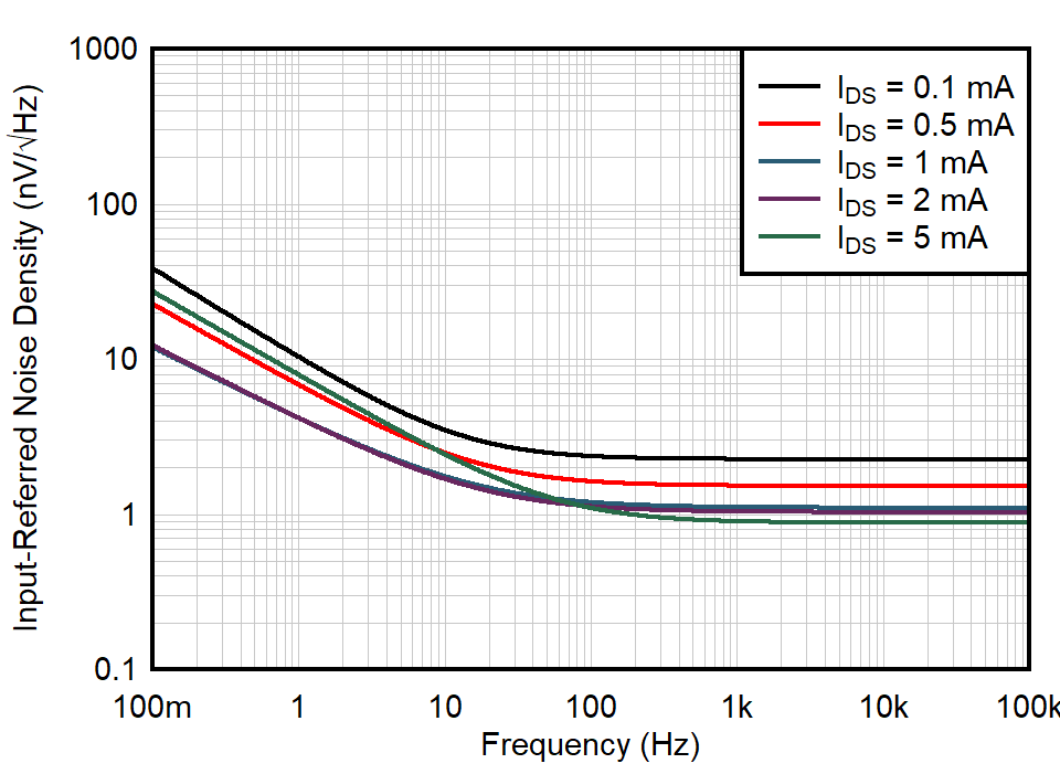
The JFE2140 is a Burr-Brown™ Audio, matched-pair discrete JFET built using Texas Instruments' modern, high-performance, analog bipolar process. The JFE2140 features performance not previously available in older discrete JFET technologies. The JFE2140 offers excellent noise performance across all current ranges, where the quiescent current can be set by the user from 50 μA to 20 mA. When biased at 5 mA, the device yields 0.9 nV/√Hz of input-referred noise, giving ultra-low noise performance with extremely high input impedance (> 1 TΩ). In addition, the matching between JFETs is tested to ±4 mV, providing low offset and high CMRR performance for differential pair configurations. The JFE2140 also features integrated diodes connected to separate clamp nodes to provide protection without the addition of high leakage, nonlinear external diodes.
The JFE2140 can withstand a high drain-to-source voltage of 40‑V, as well as gate-to-source and gate-to-drain voltages down to –40 V. The temperature range is specified from –40°C to +125°C.
| PART NUMBER | PACKAGE(1) | PACKAGE SIZE(2) |
|---|---|---|
| JFE2140 | D (SOIC, 8) | 4.9 mm × 6 mm |
| DSG (WSON, 8) | 2 mm × 2 mm |
| PARAMETER | VALUE | |
|---|---|---|
| VGSS | Gate-to-source breakdown voltage | –40 V |
| VDSS | Drain-to-source breakdown voltage | ±40 V |
| CISS | Input capacitance | 13 pF |
| VGS1 – VGS2 | Differential gate-to-source voltage matching (max) | ±4 mV |
| TJ | Junction temperature | –40°C to +125°C |
| IDSS | Drain-to-source saturation current | 18 mA |
 Simplified Schematic
 Ultra-Low Input Voltage Noise