-
LDC1001-Q1 Inductance to Digital Converter
- 1 Features
- 2 Applications
- 3 Description
- 4 Revision History
- 5 Pin Configuration and Functions
- 6 Specifications
-
7 Detailed Description
- 7.1 Overview
- 7.2 Functional Block Diagram
- 7.3 Feature Description
- 7.4 Device Functional Modes
- 7.5 Programming
- 7.6
Register Map
- 7.6.1
Register Description
- 7.6.1.1 Revision ID (offset = 0x00) [reset = 0x80]
- 7.6.1.2 Rp_MAX (offset = 0x01) [reset = 0x0E]
- 7.6.1.3 Rp_MIN (offset = 0x02) [reset = 0x14]
- 7.6.1.4 Sensor Frequency (offset = 0x03) [reset = 0x45]
- 7.6.1.5 LDC Configuration (offset = 0x04) [reset = 0x1B]
- 7.6.1.6 Clock Configuration (offset = 0x05) [reset = 0x01]
- 7.6.1.7 Comparator Threshold High LSB (offset = 0x06) [reset = 0xFF]
- 7.6.1.8 Comparator Threshold High MSB (offset = 0x07) [reset = 0xFF]
- 7.6.1.9 Comparator Threshold Low LSB (offset = 0x08) [reset = 0x00]
- 7.6.1.10 Comparator Threshold Low MSB (offset = 0x09) [reset = 0x00]
- 7.6.1.11 INTB Pin Configuration (offset = 0x0A) [reset = 0x00]
- 7.6.1.12 Power Configuration (offset = 0x0B) [reset = 0x00]
- 7.6.1.13 Status (offset = 0x20) [reset = NA]
- 7.6.1.14 Proximity Data LSB (offset = 0x21) [reset = NA]
- 7.6.1.15 Proximity Data MSB (offset = 0x22) [reset = NA]
- 7.6.1.16 Frequency Counter LSB (offset = 0x23) [reset = NA]
- 7.6.1.17 Frequency Counter Mid-Byte (offset = 0x24) [reset = NA]
- 7.6.1.18 Frequency Counter MSB (offset = 0x25) [reset = NA]
- 7.6.1
Register Description
- 8 Application and Implementation
- 9 Power Supply Recommendations
- 10Layout
- 11Device and Documentation Support
- 12Mechanical, Packaging, and Orderable Information
- IMPORTANT NOTICE
Package Options
Mechanical Data (Package|Pins)
- PW|16
Thermal pad, mechanical data (Package|Pins)
Orderable Information
LDC1001-Q1 Inductance to Digital Converter
1 Features
- AEC-Q100 Qualified for Automotive Applications:
- Temperature grade 0: –40°C to 150°C, TA
- Magnet-free operation
- Sub-micron precision
- Adjustable sensing range (through coil design)
- Lower system cost
- Remote sensor placement (decoupling the LDC from harsh environments)
- High durability (by virtue of contact-less operation)
- Insensitivity to environmental interference (such as dirt, dust, water, oil)
- Supply voltage, analog: 4.75 V to 5.25 V
- Supply voltage, IO: 1.8 V to 5.25 V
- Supply current (without LC tank): 1.7 mA
- RP resolution: 16-bit
- L resolution: 24-bit
- LC frequency range: 5 kHz to 5 MHz
2 Applications
- Touch buttons
- Angular position sensing
- Linear position sensing
- Metal proximity sensing
3 Description
The LDC1001-Q1 device is a 4.75-V to 5.25-V automotive-qualified inductance-to-digital converter designed for parallel resistance (Rp) and inductance (L) measurements. Inductive sensing technology enables precise measurement of linear or angular position of metal targets in automotive and industrial applications.
Inductive sensing is a contactless, short-range sensing technology that can enable high-resolution sensing of conductive targets in the presence of dust, dirt, oil, and moisture, which can be used by applications in harsh environments.
The LDC1001-Q1 system consists of an inductive sensor, typically a PCB coil, and a conductive target.
The LDC1001-Q1 is available in a 16-pin TSSOP package and offers several modes of operation. A serial peripheral interface (SPI) simplifies connection to an MCU.
Device Information(1)
| PART NUMBER | PACKAGE | BODY SIZE (NOM) |
|---|---|---|
| LDC1001-Q1 | TSSOP (16) | 5.00 mm × 4.40 mm |
- For all available packages, see the orderable addendum at the end of the data sheet.
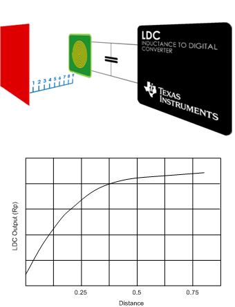
Typical Application — Axial Distance Sensing

4 Revision History
| DATE | VERSION | NOTES |
|---|---|---|
| November 2019 | * | Initial release. |