SNOSCZ6 April 2016 LDC1312-Q1 , LDC1314-Q1
PRODUCTION DATA.
- 1 Features
- 2 Applications
- 3 Description
- 4 Revision History
- 5 Description Continued
- 6 Pin Configuration and Functions
- 7 Specifications
-
8 Detailed Description
- 8.1 Overview
- 8.2 Functional Block Diagram
- 8.3 Feature Description
- 8.4 Device Functional Modes
- 8.5 Programming
- 8.6
Register Maps
- 8.6.1 Register List
- 8.6.2 Address 0x00, DATA_CH0
- 8.6.3 Address 0x02, DATA_CH1
- 8.6.4 Address 0x04, DATA_CH2 (LDC1314 only)
- 8.6.5 Address 0x06, DATA_CH3 (LDC1314 only)
- 8.6.6 Address 0x08, RCOUNT_CH0
- 8.6.7 Address 0x09, RCOUNT_CH1
- 8.6.8 Address 0x0A, RCOUNT_CH2 (LDC1314 only)
- 8.6.9 Address 0x0B, RCOUNT_CH3 (LDC1314 only)
- 8.6.10 Address 0x0C, OFFSET_CH0
- 8.6.11 Address 0x0D, OFFSET_CH1
- 8.6.12 Address 0x0E, OFFSET_CH2 (LDC1314 only)
- 8.6.13 Address 0x0F, OFFSET_CH3 (LDC1314 only)
- 8.6.14 Address 0x10, SETTLECOUNT_CH0
- 8.6.15 Address 0x11, SETTLECOUNT_CH1
- 8.6.16 Address 0x12, SETTLECOUNT_CH2 (LDC1314 only)
- 8.6.17 Address 0x13, SETTLECOUNT_CH3 (LDC1314 only)
- 8.6.18 Address 0x14, CLOCK_DIVIDERS_CH0
- 8.6.19 Address 0x15, CLOCK_DIVIDERS_CH1
- 8.6.20 Address 0x16, CLOCK_DIVIDERS_CH2 (LDC1314 only)
- 8.6.21 Address 0x17, CLOCK_DIVIDERS_CH3 (LDC1314 only)
- 8.6.22 Address 0x18, STATUS
- 8.6.23 Address 0x19, ERROR_CONFIG
- 8.6.24 Address 0x1A, CONFIG
- 8.6.25 Address 0x1B, MUX_CONFIG
- 8.6.26 Address 0x1C, RESET_DEV
- 8.6.27 Address 0x1E, DRIVE_CURRENT_CH0
- 8.6.28 Address 0x1F, DRIVE_CURRENT_CH1
- 8.6.29 Address 0x20, DRIVE_CURRENT_CH2 (LDC1314 only)
- 8.6.30 Address 0x21, DRIVE_CURRENT_CH3 (LDC1314 only)
- 8.6.31 Address 0x7E, MANUFACTURER_ID
- 8.6.32 Address 0x7F, DEVICE_ID
- 9 Application and Implementation
- 10Power Supply Recommendations
- 11Layout
- 12Device and Documentation Support
- 13Mechanical, Packaging, and Orderable Information
Package Options
Mechanical Data (Package|Pins)
- DNT|12
Thermal pad, mechanical data (Package|Pins)
Orderable Information
9 Application and Implementation
NOTE
Information in the following applications sections is not part of the TI component specification, and TI does not warrant its accuracy or completeness. TI’s customers are responsible for determining suitability of components for their purposes. Customers should validate and test their design implementation to confirm system functionality.
9.1 Application Information
9.1.1 Theory of Operation
9.1.1.1 Conductive Objects in an EM Field
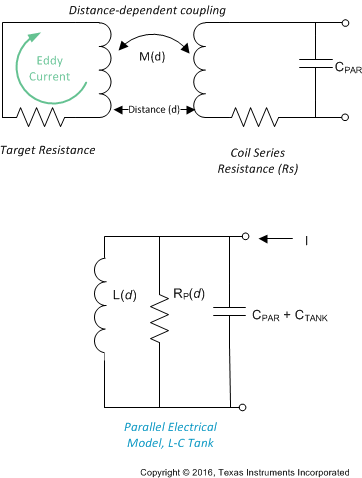
An AC current flowing through an inductor will generate an AC magnetic field. If a conductive material, such as a metal object, is brought into the vicinity of the inductor, the magnetic field will induce a circulating current (eddy current) on the surface of the conductor.
 Figure 49. Conductor in AC Magnetic Field
The eddy current is a function of the distance, size, and composition of the conductor. The eddy current generates its own magnetic field, which opposes the original field generated by the sensor inductor. This effect is equivalent to a set of coupled inductors, where the sensor inductor is the primary winding and the eddy current in the target object represents the secondary inductor. The coupling between the inductors is a function of the sensor inductor, and the resistivity, distance, size, and shape of the conductive target. The resistance and inductance of the secondary winding caused by the eddy current can be modeled as a distance dependent resistive and inductive component on the primary side (coil). Figure 49 shows a simplified circuit model of the sensor and the target as coupled coils.
9.1.1.2 L-C Resonators
An EM field can be generated using an L-C resonator, or L-C tank. One topology for an L-C tank is a parallel R-L-C construction, as shown in Figure 50.
 Figure 50. Electrical Model of the L-C Tank Sensor
An oscillator can be constructed by combining a frequency selective circuit (resonator) with a gain block in a closed loop. The criteria for oscillation are: (1) loop gain > 1, and (2) closed loop phase shift of 2π radians. The R-L-C resonator provides the frequency selectivity and contributes to the phase shift. At resonance, the impedance of the reactive components (L and C) cancels, leaving only RP, the lossy (resistive) element in the circuit. The voltage amplitude is maximized. The RP can be used to determine the sensor drive current. A lower RP requires a larger sensor current to maintain a constant oscillation amplitude. The sensor oscillation frequency is given by:

where
- C is the sensor capacitance (CTANK + CPAR)
- L is the inductance
- Q is the quality factor of the resonator. Q can be approximated by:

where
- RS is the AC series resistance of the inductor
Texas Instruments' WEBENCH design tool can be used for coil design, in which the parameter values for RP, L and C are calculated. See http://www.ti.com/webench.
RP is a function of target distance, target material, and sensor characteristics. Figure 51 shows that RP is directly proportional to the distance between the sensor and the target. The graph represents a 14-mm diameter PCB coil (23 turns, 4-mil trace width, 4-mil spacing between traces, 1-oz copper thickness, FR4).
 Figure 51. Example RP vs. Distance with a 14-mm PCB Coil and 2mm Thick Stainless Steel Target
It is important to configure the LDC current drive so that the sensor will still oscillate at the minimum RP value. For example, if the closest target distance in a system with the response shown in Figure 51 is 1mm, then the LDC RP value is 5 kΩ. The objective is to maintain a sufficient sensor oscillation voltage so that the sensor frequency can be measured even at the minimum operating distance. See section Current Drive Control Registers for details on setting the current drive.
The inductance that is measured by the LDC is

where
- L(d) is the measured sensor inductance, for a distance d between the sensor coil and target
- Linf is the inductance of the sensing coil without a conductive target (target at infinite distance)
- M(d) is the mutual inductance
- fSENSOR = sensor oscillation frequency for a distance d between the sensor coil and target
- C = CTANK + CPAR
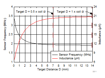
Figure 52 shows an example of variation in sensor frequency and inductance as a function of distance for a 14-mm diameter PCB coil (23 turns, 4-mil trace width, 4-mil spacing between traces, 1-oz copper thickness, FR4).
 Figure 52. Example Sensor Frequency, Inductance vs. Target Distance
 with 14-mm PCB Coil and 1.5 mm Thick Aluminum Target
In the absence of magnetic materials, such as ferrous metals and ferrites, the inductance shift, and therefore the measured frequency shift, depends only on current flow geometries. Temperature drift is dominated by physical expansion of the inductor and other mechanical system components over temperature which alter current flow geometries. Note that the additional temperature drift of the sensor capacitor must also be taken into account.
For additional information on temperature effects and temperature compensation, see LDC1000 Temperature Compensation (SNAA212)
9.2 Typical Application
Example of a multi-channel implementation using the LDC1312. This example is representative of an axial displacement application, in which the target movement is perpendicular to the plane of the coil. The second channel can be used to sense proximity of a second target, or it can be used for temperature compensation by connecting a reference coil.
 Figure 53. Example Multi-Channel Application - LDC1312
9.2.1 Design Requirements
- Design example in which Sensor 0 is used for proximity measurement and Sensor 1 is used for temperature compensation:
- Using WEBENCH for coil design
- Target distance = 0.1 cm
- Distance resolution = 0.2 µm
- Target diameter = 1 cm
- Target material = stainless steel (SS416)
- Number of PCB layers for the coil = 2
- The application requires 500SPS ( TSAMPLE = 2000 µs)
9.2.2 Detailed Design Procedure
The target distance, resolution and diameter are used as inputs to WEBENCH to design the sensor coil, The resulting coil design is a 2 layer coil, with an area of 2.5 cm2, diameter of 1.77 cm, and 39 turns. The values for RP, L and C are: RP = 6.6 kΩ, L = 43.9 µH, C = 100 pF.
Using L and C, fSENSOR = 1/2π√(LC) = 1/2π√(43.9*10-6 * 100*10-12) = 2.4 MHz
Using a system master clock of 40 MHz applied to the CLKIN pin allows flexibility for setting the internal clock frequencies. The sensor coil is connected to channel 0 (IN0A and IN0B pins).
After powering on the LDC, it will be in Sleep Mode. Program the registers as follows (example sets registers for channel 0 only; channel 1 registers can use equivalent configuration):
- Set the dividers for channel 0.
- Because the sensor freqeuncy is less than 8.75 MHz, the sensor divider can be set to 1, which means setting field CH0_FIN_DIVIDER to 0x1. By default, fIN0 = fSENSOR = 2.4MHz.
- The design constraint for fREF0 is > 4 × fSENSOR. A 20 MHz reference frequency satisfies this constraint, so the reference divider should be set to 2. This is done by setting the CH0_FREF_DIVIDER field to 0x02.
- The combined value for Chan. 0 divider register (0x14) is 0x1002.
- Program the settling time for Channel 0. The calculated Q of the coil is 10 (see Multi-Channel and Single Channel Operation).
- CH0_SETTLECOUNT ≥ Q × fREF0 / (16 × fSENSOR0) → 5.2, rounded up to 6. To provide margin to account for system tolerances, a higher value of 10 is chosen.
- Register 0x10 should be programmed to a minimum of 10.
- The settle time is: (10 x 16)/20,000,000 = 8 µs
- The value for Chan. 0 SETTLECOUNT register (0x10) is 0x000A.
- The channel switching delay is ~1μs for fREF = 20 MHz (see Multi-Channel and Single Channel Operation)
- Set the conversion time by the programming the reference count for Channel 0. The budget for the conversion time is : TSAMPLE – settling time – channel switching delay = 1000 – 8 – 1 = 991 µs
- To determine the conversion time register value, use the following equation and solve for CH0_RCOUNT: Conversion Time (tC0)= (CH0_RCOUNTˣ16)/fREF0.
- This results in CH0_RCOUNT having a value of 1238 decimal (rounded down)
- Set the CH0_RCOUNT register (0x08) to 0x04D6.
- Use the default values for the ERROR_CONFIG register (address 0x19). By default, no interrupts are enabled
- Sensor drive current: to set the CH0_IDRIVE field value, read the value from Table 10 using RP = 6.6 kΩ. In this case the IDRIVE value should be set to 18 (decimal). The INIT_DRIVE current field should be set to 0x00. The combined value for the DRIVE_CURRENT_CH0 register (addr 0x1E) is 0x9000.
- Program the MUX_CONFIG register
- Set the AUTOSCAN_EN to b1 bit to enable sequential mode
- Set RR_SEQUENCE to b00 to enable data conversion on two channels (channel 0, channel 1)
- Set DEGLITCH to b100 to set the input deglitch filter bandwidth to 3.3MHz, the lowest setting that exceeds the oscillation tank frequency.
- The combined value for the MUX_CONFIG register (address 0x1B) is 0x820C
- Finally, program the CONFIG register as follows:
- Set the ACTIVE_CHAN field to b00 to select channel 0.
- Set SLEEP_MODE_EN field to b0 to enable conversion.
- Set RP_OVERRIDE_EN to b1 to disable auto-calibration.
- Set SENSOR_ACTIVATE_SEL = b0, for full current drive during sensor activation
- Set the AUTO_AMP_DIS field to b1 to disable auto-amplitude correction
- Set the REF_CLK_SRC field to b1 to use the external clock source.
- Set the other fields to their default values.
- The combined value for the CONFIG register (address 0x1A) is 0x1601.
We then read the conversion results for channel 0 and channel 1 every 1000 µs from register addresses 0x00 and 0x02.
9.2.2.1 Recommended Initial Register Configuration Values
Based on the example configuration in section Detailed Design Procedure, the following register write sequence is recommended:
Table 44. Recommended Initial Register Configuration Values (Single-channel Operation)
| Address | Value | Register Name | Comments |
|---|---|---|---|
| 0x08 | 0x04D6 | RCOUNT_CH0 | Reference count calculated from timing requirements (1 kSPS) and resolution requirements |
| 0x10 | 0x000A | SETTLECOUNT_CH0 | Minimum settling time for chosen sensor |
| 0x14 | 0x1002 | CLOCK_DIVIDERS_CH0 | CH0_FIN_DIVIDER = 1, CH0_FREF_DIVIDER = 2 |
| 0x19 | 0x0000 | ERROR_CONFIG | Can be changed from default to report status and error conditions |
| 0x1B | 0x020C | MUX_CONFIG | Enable Ch 0 (continuous mode), set Input deglitch bandwidth to 3.3MHz |
| 0x1E | 0x9000 | DRIVE_CURRENT_CH0 | Sets sensor drive current on ch 0 |
| 0x1A | 0x1601 | CONFIG | Select active channel = ch 0, disable auto-amplitude correction and auto-calibration, enable full current drive during sensor activation, select external clock source, wake up device to start conversion. This register write must occur last because device configuration is not permitted while the LDC is in active mode. |
Table 45. Recommended Initial Register Configuration Values (Multi-channel Operation)
| Address | Value | Register Name | Comments |
|---|---|---|---|
| 0x08 | 0x04D6 | RCOUNT_CH0 | Reference count calculated from timing requirements (1 kSPS) and resolution requirements |
| 0x09 | 0x04D6 | RCOUNT_CH1 | Reference count calculated from timing requirements (1 kSPS) and resolution requirements |
| 0x10 | 0x000A | SETTLECOUNT_CH0 | Minimum settling time for chosen sensor |
| 0x11 | 0x000A | SETTLECOUNT_CH1 | Minimum settling time for chosen sensor |
| 0x14 | 0x1002 | CLOCK_DIVIDERS_CH0 | CH0_FIN_DIVIDER = 1, CH0_FREF_DIVIDER = 2 |
| 0x15 | 0x1002 | CLOCK_DIVIDERS_CH1 | CH1_FIN_DIVIDER = 1, CH1_FREF_DIVIDER = 2 |
| 0x19 | 0x0000 | ERROR_CONFIG | Can be changed from default to report status and error conditions |
| 0x1B | 0x820C | MUX_CONFIG | Enable Ch 0 and Ch 1 (sequential mode), set Input deglitch bandwidth to 3.3MHz |
| 0x1E | 0x9000 | DRIVE_CURRENT_CH0 | Sets sensor drive current on ch 0 |
| 0x1F | 0x9000 | DRIVE_CURRENT_CH1 | Sets sensor drive current on ch 1 |
| 0x1A | 0x1601 | CONFIG | disable auto-amplitude correction and auto-calibration, enable full current drive during sensor activation, select external clock source, wake up device to start conversion. This register write must occur last because device configuration is not permitted while the LDC is in active mode. |
9.2.2.2 Inductor Self-Resonant Frequency
Every inductor has a distributed parasitic capacitance, which is dependent on construction and geometry. At the Self-Resonant Frequency (SRF), the reactance of the inductor cancels the reactance of the parasitic capacitance. Above the SRF, the inductor will electrically appear to be a capacitor. Because the parasitic capacitance is not well-controlled or stable, TI recommends that: fSENSOR < 0.8 × fSR.
 Figure 54. Example Coil Inductance vs. Frequency
In Figure 54, the inductor has a SRF at 6.38 MHz; therefore the inductor should not be operated above 0.8×6.38 MHz, or 5.1 MHz.
9.2.3 Application Curves
Common test conditions (unless specified otherwise):
- Sensor inductor: 2 layer, 32 turns/layer, 14mm diameter, PCB inductor with L=19.4 µH, RP=5.7 kΩ at 2 MHz
- Sensor capacitor: 330pF 1% COG/NP0
- Target: Aluminum, 1.5 mm thickness
- Channel = Channel 0 (continuous mode)
- CLKIN = 40MHz, CHx_FIN_DIVIDER = 0x01, CHx_FREF_DIVIDER = 0x001
- CH0_RCOUNT = 0xFFFF, SETTLECOUNT_CH0 = 0x0100
- RP_OVERRIDE = 1, AUTO_AMP_DIS = 1, DRIVE_CURRENT_CH0 = 0x9800
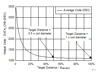
 Figure 55. Typical Output Code vs. Target Distance (0 to 14mm)
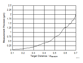
 Figure 56. Measurement precision in Distance vs. Target Distance (0 to 10mm)