SNOSDC7B December 2021 – December 2021 LDC3114-Q1
PRODUCTION DATA
- 1 Features
- 2 Applications
- 3 Description
- 4 Revision History
- 5 Pin Configuration and Functions
- 6 Specifications
-
7 Detailed Description
- 7.1 Overview
- 7.2 Functional Block Diagram
- 7.3 Feature Description
- 7.4 Device Functional Modes
- 7.5 Register Maps
-
8 Application and Implementation
- 8.1
Application Information
- 8.1.1 Theory of Operation
- 8.1.2 Designing Sensor Parameters
- 8.1.3 Setting COM Pin Capacitor
- 8.1.4 Defining Power-On Timing
- 8.1.5 Configuring Button or Raw Data Scan Rate
- 8.1.6 Programming Button or Raw Data Sampling Window
- 8.1.7 Scaling Frequency Counter Output
- 8.1.8 Setting Button Triggering Threshold
- 8.1.9 Tracking Baseline
- 8.1.10 Mitigating False Button Detections
- 8.1.11 Reporting Interrupts for Button Presses, Raw Data Ready and Error Conditions
- 8.1.12 Estimating Supply Current
- 8.2 Typical Application
- 8.1
Application Information
- 9 Power Supply Recommendations
- 10Layout
- 11Device and Documentation Support
- 12Mechanical, Packaging, and Orderable Information
Package Options
Mechanical Data (Package|Pins)
- PW|16
Thermal pad, mechanical data (Package|Pins)
Orderable Information
8.1.8 Setting Button Triggering Threshold
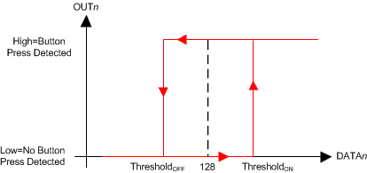
Every material shows some hysteresis when the material deforms then returns to the original state. The amount of hysteresis is a function of material properties and physical parameters, such as size and thickness. This feature modifies the hysteresis of the button signal threshold according to different materials and various button shapes and sizes. Hysteresis can be programmed in Register HYST (Address 0x18). By default, the button triggering hysteresis is set to 32. The nominal button triggering threshold is 128. With hysteresis, the effective on-threshold is 128 + 32 = 160. This means if the DATAn (n = 0, 1, 2, or 3) reaches 160, the LDC3114-Q1 considers that as a button press. When the DATAn decreases to 128 – 32 = 96, the LDC considers the button to be released.


 Figure 8-8 Button Triggering Threshold with Hysteresis. Output Polarity: Active High