SNOSDI7 December   2023 LDC5071-Q1

PRODUCTION DATA  

  1.   1
  2. Features
  3. Applications
  4. Description
  5. Pin Configuration and Functions
  6. Specifications
    1. 5.1 Absolute Maximum Ratings
    2. 5.2 ESD Ratings
    3. 5.3 Recommended Operating Conditions
    4. 5.4 Thermal Information
    5. 5.5 Electrical Characteristics
    6. 5.6 Diagnostics
    7. 5.7 Switching Characteristics
    8. 5.8 Typical Characteristics
  7. Detailed Description
    1. 6.1 Overview
    2. 6.2 Functional Block Diagram
    3. 6.3 Feature Description
      1. 6.3.1 Input Supply Voltage
      2. 6.3.2 Excitation Signal
      3. 6.3.3 Signal Processing Block
        1. 6.3.3.1 Demodulation
        2. 6.3.3.2 Fixed Gain Control
        3. 6.3.3.3 Automatic Gain Control
      4. 6.3.4 Output Stage
      5. 6.3.5 Diagnostics
        1. 6.3.5.1 Undervoltage Diagnostics
        2. 6.3.5.2 Initialization Diagnostics
        3. 6.3.5.3 Normal State Diagnostics
        4. 6.3.5.4 Fault State Diagnostics
    4. 6.4 Device Functional Modes
      1. 6.4.1 IDLE State
      2. 6.4.2 DIAGNOSTICS State
      3. 6.4.3 NORMAL State
      4. 6.4.4 FAULT State
      5. 6.4.5 DISABLED State
  8. Application and Implementation
    1. 7.1 Application Information
    2. 7.2 Typical Applications
      1. 7.2.1 5-V Supply Mode
        1. 7.2.1.1 Design Requirements
        2. 7.2.1.2 Detailed Design Procedure
          1. 7.2.1.2.1 VREG and VCC
          2. 7.2.1.2.2 Output Capacitors
          3. 7.2.1.2.3 Automatic Gain Control (AGC) Mode
        3. 7.2.1.3 Application Curve
      2. 7.2.2 3.3-V Supply Mode
        1. 7.2.2.1 Design Requirements
        2. 7.2.2.2 Detailed Design Procedure
          1. 7.2.2.2.1 VREG and VCC
          2. 7.2.2.2.2 Output Capacitors
          3. 7.2.2.2.3 Fixed Gain Mode
      3. 7.2.3 Redundancy Mode
      4. 7.2.4 Single-Ended Mode
      5. 7.2.5 External Diagnostics Required for Loss of VCC or GND
    3. 7.3 Power Supply Recommendations
      1. 7.3.1 Mode 1: VCC = 5 V, VREG = 3.3 V
      2. 7.3.2 Mode 2: VCC = VREG = 3.3 V
    4. 7.4 Layout
      1. 7.4.1 Layout Guidelines
      2. 7.4.2 Layout Example
  9. Device and Documentation Support
    1. 8.1 Receiving Notification of Documentation Updates
    2. 8.2 Support Resources
    3. 8.3 Trademarks
    4. 8.4 Electrostatic Discharge Caution
    5. 8.5 Glossary
  10. Revision History
  11. 10Mechanical, Packaging, and Orderable Information

Package Options

Mechanical Data (Package|Pins)
Thermal pad, mechanical data (Package|Pins)
Orderable Information

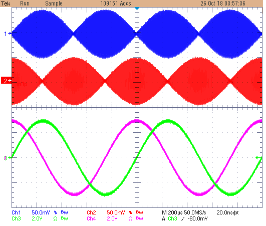
Application Curve

GUID-C14308E0-CCCB-43B7-BDF4-EF31A4A11418-low.png
CH1 = IN0P-IN0N
CH2 = IN1P-IN1N
CH3 = OUT0P-OUT0N
CH4 = OUT1P-OUT1N
Figure 7-2 INx and OUTx Signals at 1000-Hz Rotation Speed