SNOSBI3C July 2000 – October 2018 LF198-N , LF298 , LF398-N
PRODUCTION DATA.
- 1 Features
- 2 Applications
- 3 Description
- 4 Revision History
- 5 Pin Configuration and Functions
-
6 Specifications
- 6.1 Absolute Maximum Ratings
- 6.2 Recommended Operating Conditions
- 6.3 Thermal Information
- 6.4 Electrical Characteristics, LF198-N and LF298
- 6.5 Electrical Characteristics, LF198A-N
- 6.6 Electrical Characteristics, LF398-N
- 6.7 Electrical Characteristics, LF398A-N (OBSOLETE)
- 6.8 Typical Characteristics
- 7 Parameter Measurement Information
- 8 Detailed Description
-
9 Application and Implementation
- 9.1 Application Information
- 9.2
Typical Applications
- 9.2.1 X1000 Sample and Hold
- 9.2.2 Sample and Difference Circuit
- 9.2.3 Ramp Generator With Variable Reset Level
- 9.2.4 Integrator With Programmable Reset Level
- 9.2.5 Output Holds at Average of Sampled Input
- 9.2.6 Increased Slew Current
- 9.2.7 Reset Stabilized Amplifier
- 9.2.8 Fast Acquisition, Low Droop Sample and Hold
- 9.2.9 Synchronous Correlator for Recovering Signals Below Noise Level
- 9.2.10 2-Channel Switch
- 9.2.11 DC and AC Zeroing
- 9.2.12 Staircase Generator
- 9.2.13 Differential Hold
- 9.2.14 Capacitor Hysteresis Compensation
- 10Power Supply Recommendations
- 11Layout
- 12Device and Documentation Support
- 13Mechanical, Packaging, and Orderable Information
Package Options
Mechanical Data (Package|Pins)
- LMC|8
Thermal pad, mechanical data (Package|Pins)
Orderable Information
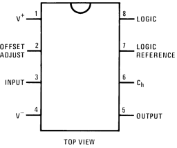
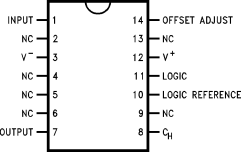
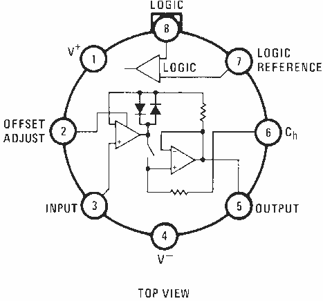
5 Pin Configuration and Functions
P Package
8-Pin PDIP
Top View

D Package
14-Pin SOIC
Top View

LMC Package
8-Pin TO-99
Top View

A military RETS electrical test specification is available on request. The LF198-N may also be procured to Standard Military Drawing #5962-8760801GA or to MIL-STD-38510 part ID JM38510/12501SGA.
Pin Functions
| PIN | TYPE(1) | DESCRIPTION | |||
|---|---|---|---|---|---|
| NAME | LF298, LF398-N | LFx98x | LF398-N | ||
| SOIC-14 | TO-99 | PDIP-8 | |||
| V+ | 12 | 1 | 1 | P | Positive supply |
| OFFSET ADJUST | 14 | 2 | 2 | A | DC offset compensation pin |
| INPUT | 1 | 3 | 3 | A | Analog Input |
| V– | 3 | 4 | 4 | P | Negative supply |
| OUTPUT | 7 | 5 | 5 | O | Output |
| Ch | 8 | 6 | 6 | A | Hold capacitor |
| LOGIC REFERENCE | 10 | 7 | 7 | I | Reference for LOGIC input |
| LOGIC | 11 | 8 | 8 | I | Logic input for Sample and Hold modes |
| NC | 2, 4, 5, 6, 9, 13 | — | — | NA | No connect |
(1) P = Power, G = Ground, I = Input, O = Output, A = Analog