SNOSD57 June 2017 LF298-MIL
PRODUCTION DATA.
- 1 Features
- 2 Applications
- 3 Description
- 4 Revision History
- 5 Pin Configuration and Functions
- 6 Specifications
- 7 Parameter Measurement Information
- 8 Detailed Description
-
9 Application and Implementation
- 9.1 Application Information
- 9.2
Typical Applications
- 9.2.1 X1000 Sample and Hold
- 9.2.2 Sample and Difference Circuit
- 9.2.3 Ramp Generator With Variable Reset Level
- 9.2.4 Integrator With Programmable Reset Level
- 9.2.5 Output Holds at Average of Sampled Input
- 9.2.6 Increased Slew Current
- 9.2.7 Reset Stabilized Amplifier
- 9.2.8 Fast Acquisition, Low Droop Sample and Hold
- 9.2.9 Synchronous Correlator for Recovering Signals Below Noise Level
- 9.2.10 2-Channel Switch
- 9.2.11 DC and AC Zeroing
- 9.2.12 Staircase Generator
- 9.2.13 Differential Hold
- 9.2.14 Capacitor Hysteresis Compensation
- 10Power Supply Recommendations
- 11Layout
- 12Device and Documentation Support
- 13Mechanical, Packaging, and Orderable Information
Package Options
Mechanical Data (Package|Pins)
- LMC|8
Thermal pad, mechanical data (Package|Pins)
Orderable Information
7 Parameter Measurement Information
7.1 TTL and CMOS 3 V ≤ VLOGIC (Hi State) ≤ 7 V
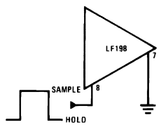
Threshold = 1.4 V
Figure 18. Sample When Logic High With TTL and CMOS Biasing
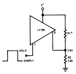
Threshold = 1.4 V
Select for 2.8 V at pin 8
Figure 19. Sample When Logic Low With TTL and CMOS Biasing
7.2 CMOS 7 V ≤ VLOGIC (Hi State) ≤ 15 V
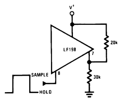
Threshold = 0.6 (V+) + 1.4 V
Figure 20. Sample When Logic High With CMOS Biasing
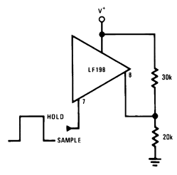
Threshold = 0.6 (V+) –1.4V
Figure 21. Sample When Logic Low With CMOS Biasing
7.3 Operational Amplifier Drive
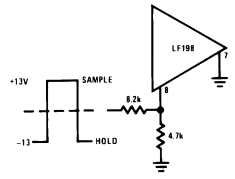
Threshold ≈ +4 V
Figure 22. Sample When Logic High With Operational Amplifier Biasing
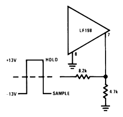
Threshold = −4 V
Figure 23. Sample When Logic Low With Operational Amplifier Biasing