SNOSBI3C July 2000 – October 2018 LF198-N , LF298 , LF398-N
PRODUCTION DATA.
- 1 Features
- 2 Applications
- 3 Description
- 4 Revision History
- 5 Pin Configuration and Functions
-
6 Specifications
- 6.1 Absolute Maximum Ratings
- 6.2 Recommended Operating Conditions
- 6.3 Thermal Information
- 6.4 Electrical Characteristics, LF198-N and LF298
- 6.5 Electrical Characteristics, LF198A-N
- 6.6 Electrical Characteristics, LF398-N
- 6.7 Electrical Characteristics, LF398A-N (OBSOLETE)
- 6.8 Typical Characteristics
- 7 Parameter Measurement Information
- 8 Detailed Description
-
9 Application and Implementation
- 9.1 Application Information
- 9.2
Typical Applications
- 9.2.1 X1000 Sample and Hold
- 9.2.2 Sample and Difference Circuit
- 9.2.3 Ramp Generator With Variable Reset Level
- 9.2.4 Integrator With Programmable Reset Level
- 9.2.5 Output Holds at Average of Sampled Input
- 9.2.6 Increased Slew Current
- 9.2.7 Reset Stabilized Amplifier
- 9.2.8 Fast Acquisition, Low Droop Sample and Hold
- 9.2.9 Synchronous Correlator for Recovering Signals Below Noise Level
- 9.2.10 2-Channel Switch
- 9.2.11 DC and AC Zeroing
- 9.2.12 Staircase Generator
- 9.2.13 Differential Hold
- 9.2.14 Capacitor Hysteresis Compensation
- 10Power Supply Recommendations
- 11Layout
- 12Device and Documentation Support
- 13Mechanical, Packaging, and Orderable Information
Package Options
Mechanical Data (Package|Pins)
Thermal pad, mechanical data (Package|Pins)
Orderable Information
9.2.1.3 Application Curves
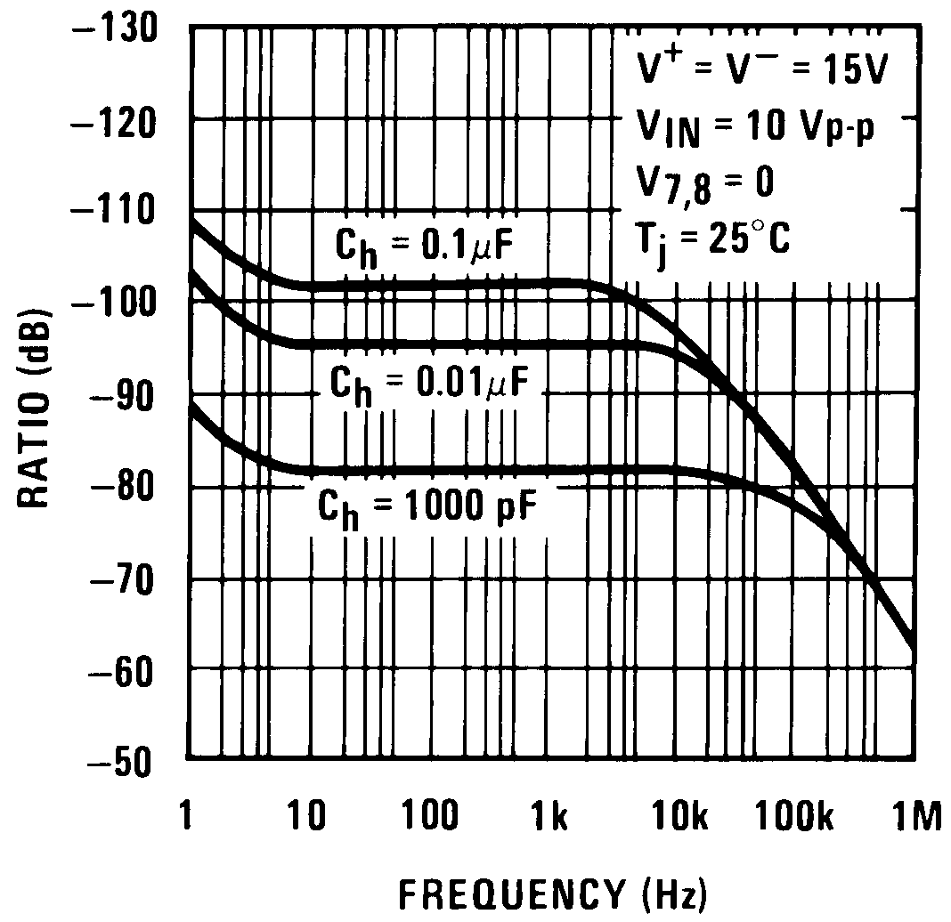
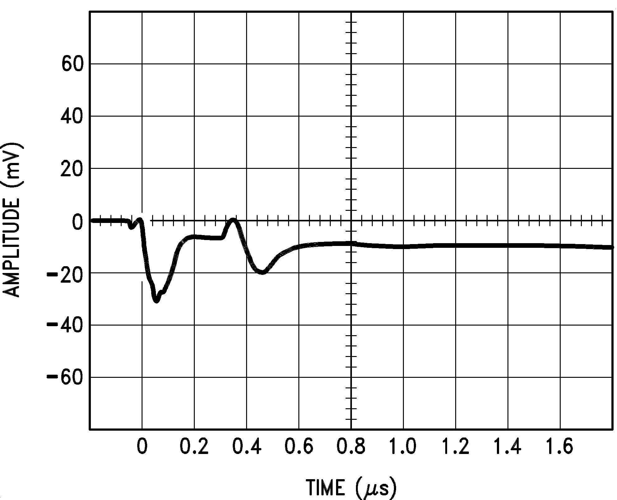
The feedthrough rejection ratio of the LF198-N is extremely good and provides good isolation for a wide variety of hold capacitors as Figure 26 shows. Additionally, the output transient settles almost completely after 0.8 µs and would be ready to sample as shown in Figure 27.
 Figure 26. Feedthrough Rejection Ratio (Hold Mode)
  Figure 27. Output Transient at Start of Hold Mode